Manufacture method of semiconductor device

A manufacturing method and semiconductor technology, applied in semiconductor/solid-state device manufacturing, electrical components, circuits, etc., can solve problems such as uneven filling of materials, achieve the effects of eliminating interlayer dielectric layer gap filling, expanding opening size, and easy deposition

Inactive Publication Date: 2011-03-23
SEMICON MFG INT (SHANGHAI) CORP +1
View PDF0 Cites 7 Cited by
  • Summary
  • Abstract
  • Description
  • Claims
  • Application Information

AI Technical Summary

Problems solved by technology

It should be noted that for the rapid development of sub-micron semiconductor devices, the distance between the gate and the gate is very narrow, at 120-160 nanometers, when the area between the gate and the gate is filled with ILD material , it is easy to cause uneven material filling and void defects. Figure 1c The void defect that appears in the middle dashed box

Method used


Image

  • Manufacture method of semiconductor device
  • Manufacture method of semiconductor device
  • Manufacture method of semiconductor device

Examples


Embodiment Construction

[0030] In order to make the object, technical solution, and advantages of the present invention clearer, the present invention will be further described in detail below with reference to the accompanying drawings and examples.

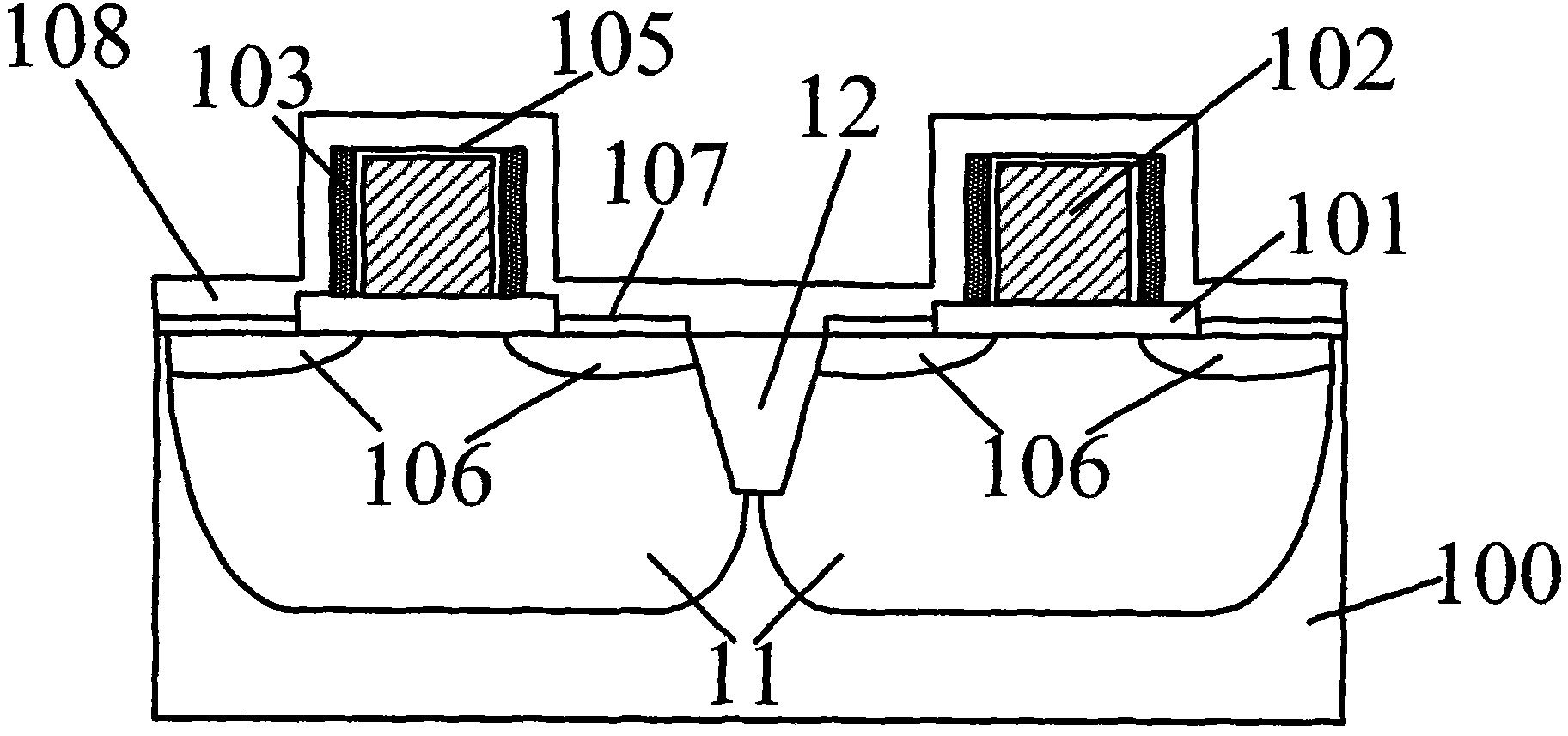
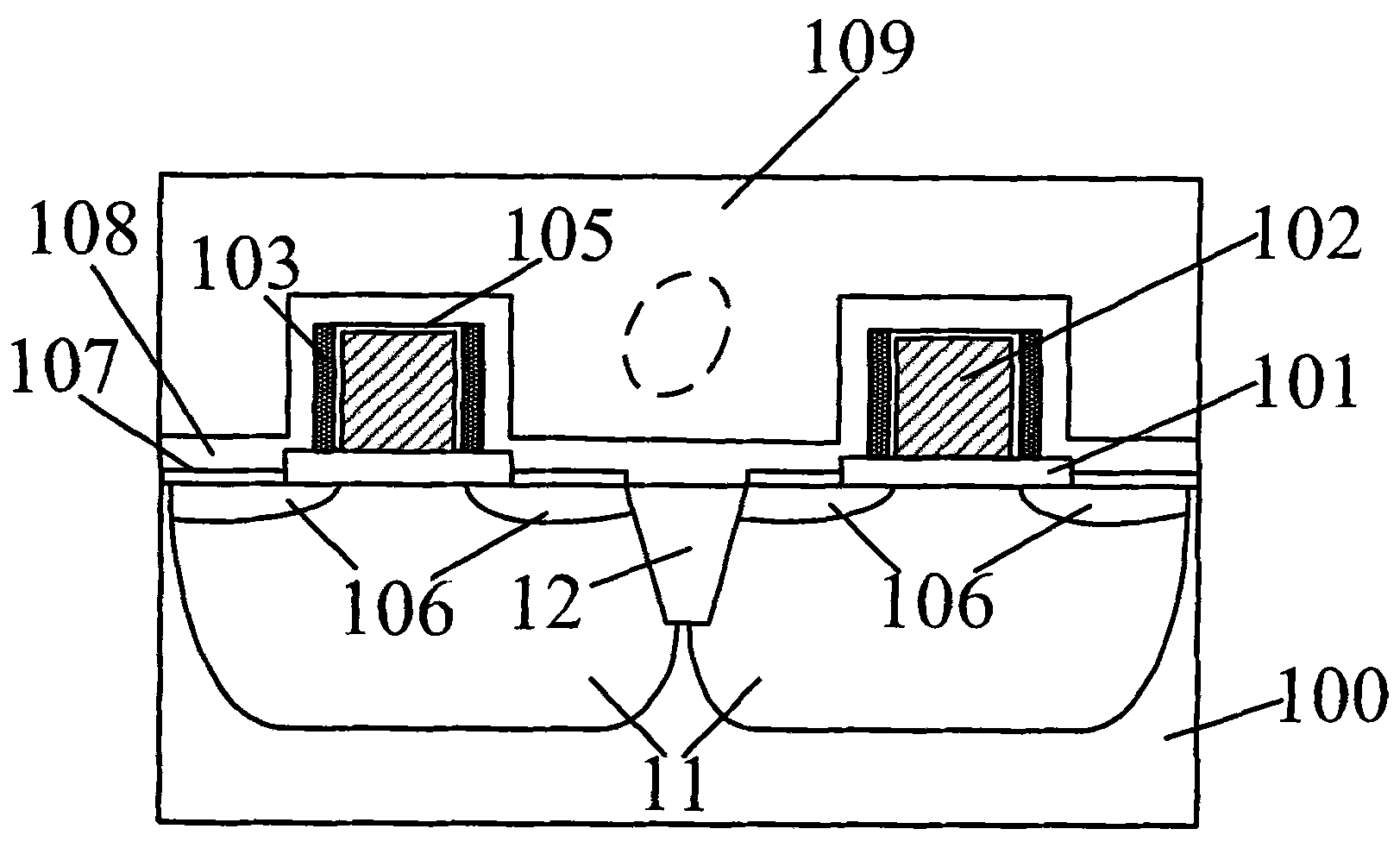
[0031] In the present invention, after etching back the nitride, the shape of the first sidewall layer is corrected so that the first sidewall layer has a tapered pointed shape. When the ILD material is deposited between the gate and the gate, the relative expansion The size of the opening between the gate and the gate is reduced, making it easier for the ILD material to be deposited in the area between the gate and the gate, thereby effectively eliminating the problem of interlayer dielectric layer gap fill (ILD gap fill).

[0032] The present invention forms the fabrication method of the semiconductor device with ILD, below in conjunction with Figures 2a to 2c Describe in detail.

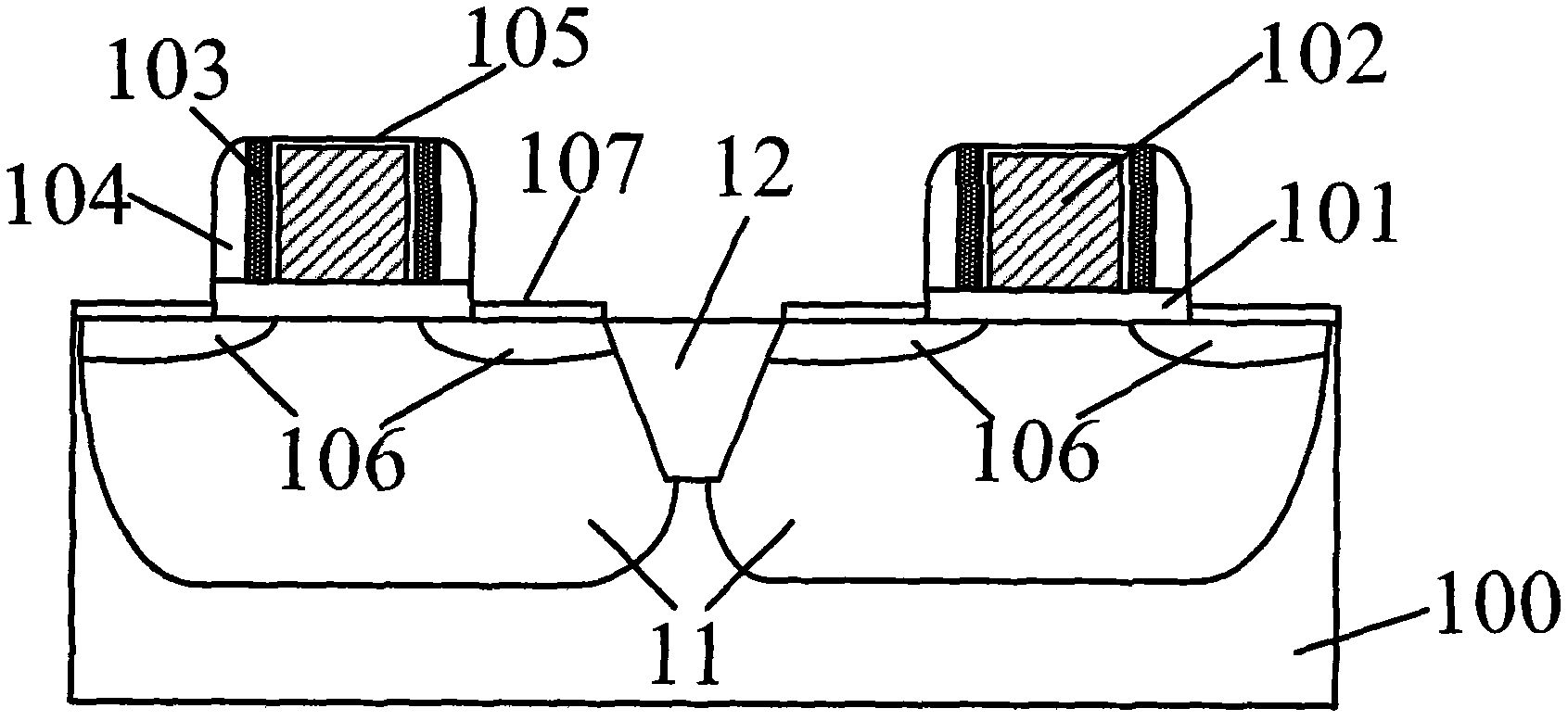
[0033] Such as Figure 2a As shown, a semiconductor substrate 100 ...


PUM


Abstract

The invention discloses a manufacture method of a semiconductor device, the semiconductor device includes a gate oxide and a gate electrode, which are orderly installed on a semiconductor substrate, a first sidewall layer located at two sides of the gate electrode and a second sidewall layer located at an external side of the first sidewall layer, the key is that the manufacture method comprises the following steps: etching away the second sidewall layer; and etching the first sidewall layer to form a conic shape. With the method, size of a gap between the gate electrodes is relatively expanded, so that an interlayer medium material can be deposited in a region between the gate electrodes more easily, and a problem of interlayer medium layer gap filling is effectively solved.

Description

technical field [0001] The invention relates to the technical field of semiconductor manufacturing, in particular to a method for manufacturing a semiconductor device. Background technique [0002] Currently, in the manufacture of semiconductor devices, silicon nitride can be used to induce stress in the transistor channel, thereby adjusting the carrier mobility in the channel. The induced stress depends on the stress state of the silicon nitride itself and the relative position of the associated channel part. The greater the stress, the greater the mobility of carriers in the channel. Moreover, silicon nitride can also be used as an etch stop layer in subsequent processes. [0003] In order to obtain a semiconductor device with a silicon nitride layer of high tensile stress, the combination Figure 1a and 1b The manufacturing method of the semiconductor device in the prior art is described in detail. [0004] Such as Figure 1a As shown, a semiconductor substrate 100 is...

Claims


Application Information

Patent Timeline
Patent Type & Authority Applications(China)
IPC IPC(8): H01L21/8234H01L21/336
Inventor 韩秋华王新鹏
Owner SEMICON MFG INT (SHANGHAI) CORP
Why Eureka
Try Eureka