Method and digital chip for generating multi-path SPWM signals

A digital chip and signal technology, applied in electrical components, pulse technology, pulse modulation, etc., can solve the problems of increased volume of frequency converter, complex software and hardware structure, and large CPU time

Inactive Publication Date: 2012-05-30
CENTRAL SOUTH UNIVERSITY OF FORESTRY AND TECHNOLOGY
View PDF0 Cites 0 Cited by
  • Summary
  • Abstract
  • Description
  • Claims
  • Application Information

AI Technical Summary

Problems solved by technology

[0005] First, the precise calculation of the trigger time needs to solve the transcendental equation, which takes up a lot of CPU time and cannot meet the real-time requirements. Usually, only approximate calculation methods can be used, and the carrier frequency is reduced to reduce the amount of calculation. Even so, a separate CPU is often required Dedicated to the calculation of trigger time
Reducing the carrier frequency makes the switching device unable to fully exert its potential, plus the calculation error of the trigger time and the time error caused by sending it to the FPGA are relatively large, resulting in an increase in the low-order harmonics of the voltage output by the inverter, requiring a large filter device These low-order harmonics can be filtered out, resulting in an increase in the size of the inverter and a decrease in performance
[0006] Second, because the calculation of the trigger time takes up a lot of CPU time, the inverter control system has to adopt a dual-CPU structure, and one of the CPUs is dedicated to the calculation of the trigger time of the SPWM signal, resulting in a very complicated system software and hardware structure and difficult maintenance.

Method used


Image

  • Method and digital chip for generating multi-path SPWM signals
  • Method and digital chip for generating multi-path SPWM signals
  • Method and digital chip for generating multi-path SPWM signals

Examples


Embodiment 1

[0060] The present invention will be further described below with reference to the accompanying drawings and embodiments. The following description is only used to understand the technical solutions of the present invention and is not used to limit the scope of the present invention.

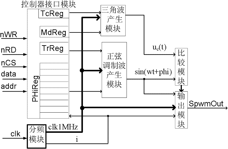
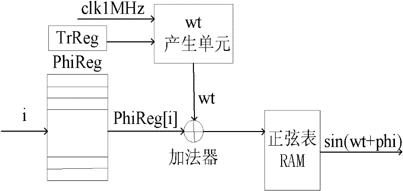
[0061] figure 1 To utilize the method for generating multiple SPWM signals and an embodiment of the digital chip disclosed in the present invention. The embodiment describes the functional block diagram of the 48-channel SPWM generator chip, which uses a 50MHz external clock signal, is designed as the trigger time error is less than 1us, and the sampling period is 1us. The 48-channel SPWM signal generator chip FPGA implementation is mainly composed of a controller interface module, a triangle wave generation module, a sine modulation wave generation module, a frequency division module, a comparison module, and an output module. The instructions are as follows:

[0062] Controller interface module: P...


PUM


Abstract

The invention discloses a method and a digital chip for generating multi-path sinusoidal pulse width modulation (SPWM) signals. The method comprises the following steps of: 1, generating an application triangular carrier, a reference triangular carrier and a multi-path sine signal value at t moment; 2, generating the multi-path SPWM signals through comparison; and 3, circulating. The digital chipcomprises a controller interface module, a triangular wave generating module, a sine modulation wave generating module, a comparison module, an output module and a frequency division module. The invention is easy to implement, the hardware resources are saved, and the triggered time error is low. A control circuit can reduce a central processing unit (CPU), software and hardware complexity of a control system is simplified, the carrier frequency is improved, the potentiality of a power switching device is fully exerted, the triggered time accuracy of the SPWM signals is improved, low-order harmonic waves are reduced, the performance of a frequency converter is improved, and the problem of insufficiency of CPU timers, pins and other hardware resources is solved.

Description

Technical field [0001] The invention belongs to the field of power electronics, and relates to a method for generating multiple SPWM signals, digital chips, high-voltage frequency converters, inverters, and the like. technical background [0002] SPWM (sinusoidal pulse width modulation, sinusoidal pulse width modulation) signal is a digital signal generated by comparing the magnitude of the sinusoidal modulation wave and the triangular carrier. When the sinusoidal modulation wave is greater than the triangular carrier, the SPWM signal is high, and vice versa. Low level. The power unit cascaded high-voltage frequency converter and inverter (hereinafter collectively referred to as the frequency converter) are composed of multiple power units, which require multiple (up to 48) SPWM signals. The conventional method of generating multiple SPWM signals is that the triangular carrier amplitude of each SPWM signal is the same, but time shifted. The amplitude and phase of the sinusoidal ...

Claims


Application Information

Patent Timeline
IPC IPC(8): H03K7/00
Inventor 王湘中朱俊杰
Owner CENTRAL SOUTH UNIVERSITY OF FORESTRY AND TECHNOLOGY
Why Eureka
Try Eureka