Check patentability & draft patents in minutes with Patsnap Eureka AI!

Semiconductor silicon wafer cleaning process chamber and cleaning method

A semiconductor and process chamber technology, which is applied to the semiconductor silicon wafer cleaning process chamber and the field of cleaning, to achieve the effects of improving the cleaning effect, reducing the liquid consumption and reducing the thickness of the boundary layer

Inactive Publication Date: 2016-04-27
SHANGHAI INTEGRATED CIRCUIT RES & DEV CENT
View PDF4 Cites 0 Cited by
  • Summary
  • Abstract
  • Description
  • Claims
  • Application Information

AI Technical Summary

Problems solved by technology

Reducing boundary layer thickness has become an important challenge to improve cleaning efficiency

Method used


Image

  • Semiconductor silicon wafer cleaning process chamber and cleaning method

Examples


Embodiment Construction

[0023] In order to better understand the technical content of the present invention, specific embodiments are given together with the attached drawings for description as follows.

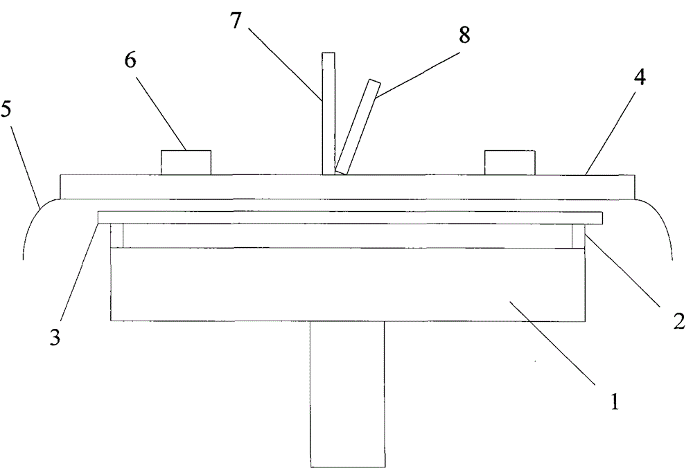
[0024] Please refer to figure 1 , figure 1 Shown is a schematic structural diagram of a cleaning process chamber for semiconductor silicon wafers according to a preferred embodiment of the present invention. The present invention provides a cleaning process chamber for semiconductor silicon wafers. Inside the process chamber, there is a platform 1 that can be lifted and rotated. Above the platform 1, there are several silicon wafer supports 2 with vacuum pipelines for carrying and fixing silicon wafers. Sheet 3, a cover plate 4 with an area larger than the silicon chip 3 is arranged above the silicon chip 3, and the cover plate 4 has one or more water outlet holes 7, which are connected to different liquid or gas pipelines 8 , the cover plate 4 is equipped with an ultrasonic oscillator 6 , the ed...


PUM


Abstract

The invention provides a semiconductor silicon wafer cleaning process cavity and a cleaning method. A platform capable of being elevated and rotated is arranged in the process cavity; multiple silicon wafer brackets attached with vacuum pipelines are arranged on the upper part of the platform and are used for loading and fixing silicon wafers; a cover plate with the area larger than those of the silicon wafers is arranged above the silicon wafers; the cover plate is provided with one or multiple water draining holes which are connected to different liquid or gas pipelines; and the edge of the cover plate is bent downwards to form a flow guide protective cover. The semiconductor silicon wafer cleaning process cavity and the cleaning method can enhance the cleaning effect and reduce the consumption of various resources in the single slice type cleaning course.

Description

technical field [0001] The invention belongs to the technical field of integrated circuit technology, and in particular relates to a novel semiconductor silicon chip cleaning process chamber and cleaning method. Background technique [0002] With the continuous progress of integrated circuit manufacturing technology, the volume of semiconductor devices is becoming smaller and smaller, which also leads to very small particles becoming enough to affect the manufacturing and performance of semiconductor devices, so the silicon wafer cleaning process has also become more and more important. [0003] At present, the cleaning method widely used in the industry is wet cleaning, that is, various chemical solutions and pure water are used to clean silicon wafers. When the chemical solution contacts the silicon wafer, there is a very thin water film on the surface of the silicon wafer. Due to the effect of intermolecular attraction, this layer of water film is stationary relative to ...

Claims


Application Information

Patent Timeline
Patent Type & Authority Patents(China)
IPC IPC(8): H01L21/00H01L21/02B08B3/12
Inventor 张晨骋
Owner SHANGHAI INTEGRATED CIRCUIT RES & DEV CENT
Features
  • R&D
  • Intellectual Property
  • Life Sciences
  • Materials
  • Tech Scout
  • Unparalleled Data Quality
  • Higher Quality Content
  • 60% Fewer Hallucinations
Learn More