TFT-LCD array substrate and method for manufacturing the same

A technology of an array substrate and a manufacturing method, applied in the field of liquid crystal display, can solve the problems of reducing the aperture ratio of the liquid crystal display device, affecting the display effect of the liquid crystal display device, etc., and achieve the effect of increasing the size and increasing the facing area.

Active Publication Date: 2011-04-20
BOE TECH GRP CO LTD +1
View PDF0 Cites 9 Cited by
  • Summary
  • Abstract
  • Description
  • Claims
  • Application Information

AI Technical Summary

Problems solved by technology

[0009] Taking the storage capacitor formed on the common electrode line as an example, in the prior art, the facing area S between the common electrode line 5 and the pixel electrode 4 is often increased by increasing the line width of the common electrode line 5 in the pixel area , so as to increase the storage capacitor Cst; however, this approach will inevitably reduce the aperture ratio of the liquid crystal display device and affect the display effect of the liquid crystal display device

Method used


Image

  • TFT-LCD array substrate and method for manufacturing the same
  • TFT-LCD array substrate and method for manufacturing the same
  • TFT-LCD array substrate and method for manufacturing the same

Examples


Embodiment 1

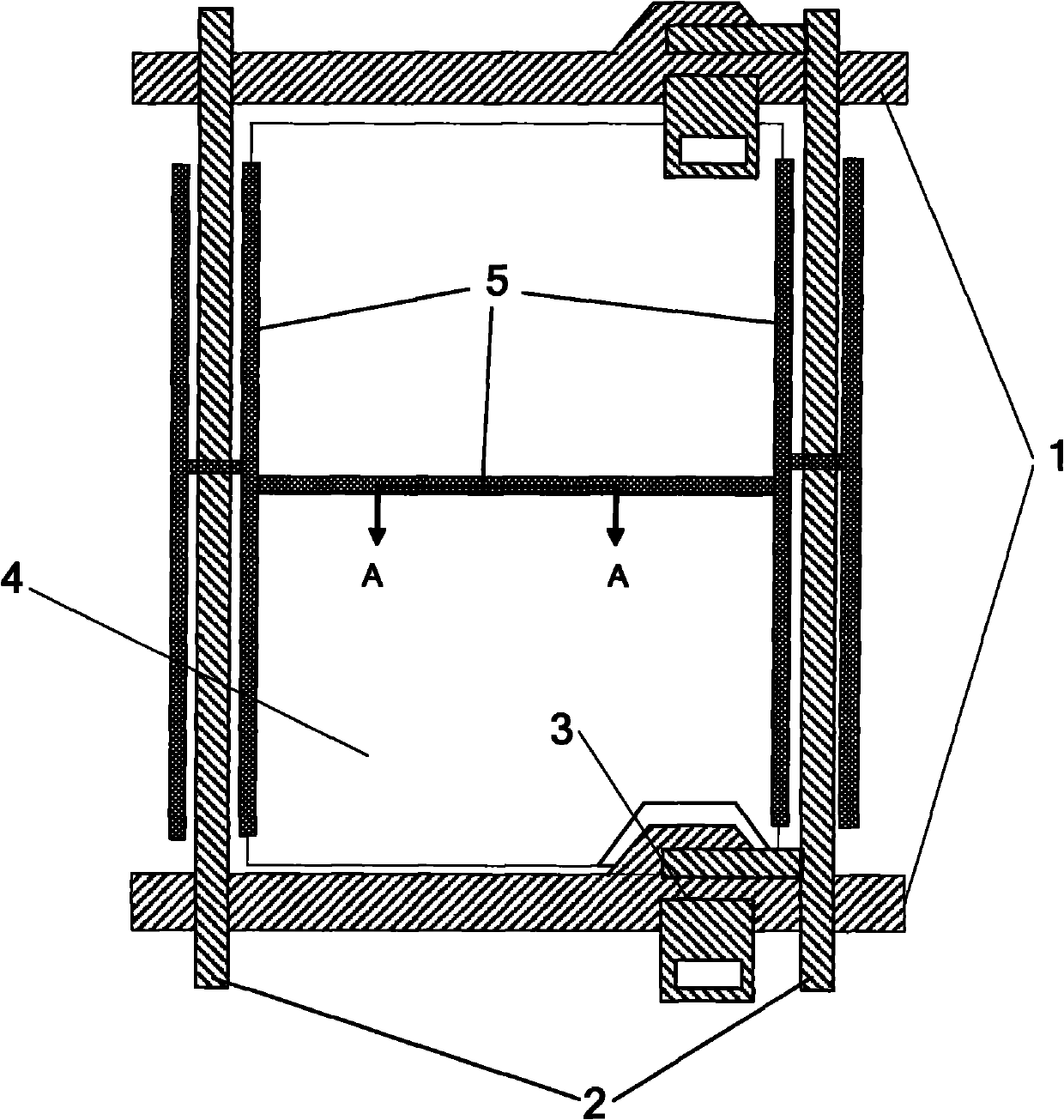
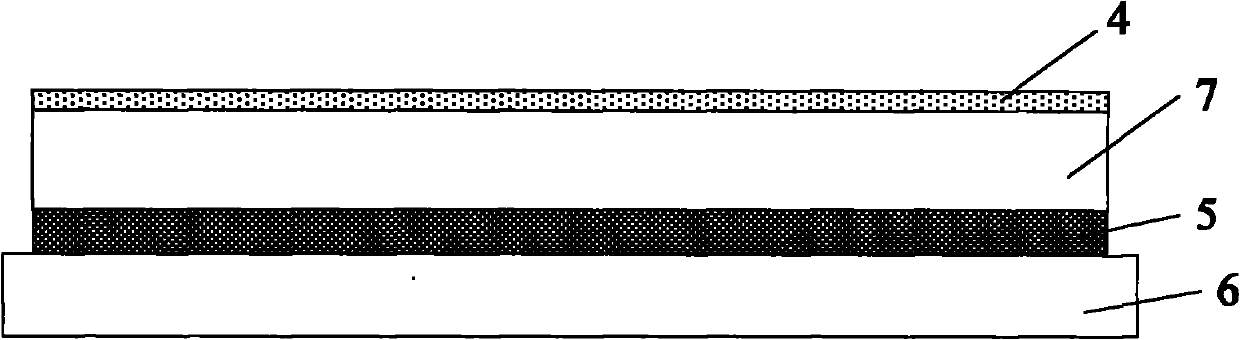
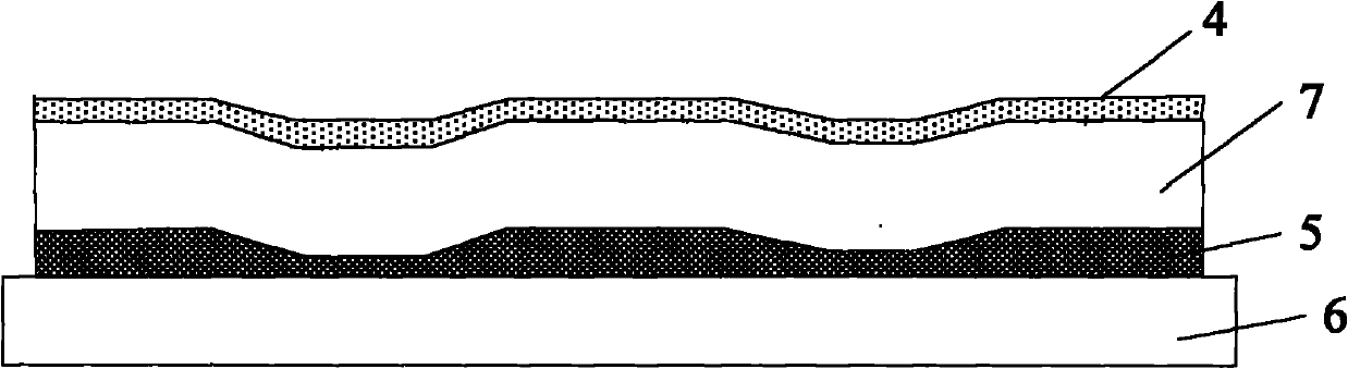
[0032] An embodiment of the present invention provides a TFT-LCD array substrate, combined with image 3 As shown, the TFT-LCD array substrate provided in this embodiment includes a glass substrate 6, and a common electrode line 5, an insulating layer 7, and a pixel electrode 4 sequentially formed on the glass substrate 6; the pixel electrode 4, the insulating layer 7, and the common The combination of the electrode lines 5 constitutes the storage capacitor Cst; in addition, a corresponding concave-convex structure is formed on the surface of the common electrode line 5 and in the region of the pixel electrode 4 facing the common electrode line 5 .

[0033] On the above-mentioned TFT-LCD array substrate, since the surface of the common electrode line 5 and the area facing the common electrode line 5 on the pixel electrode 4 are designed with corresponding concavo-convex surfaces, so that without increasing the line width It also achieves the effect of increasing the facing are...

Embodiment 2

[0041] For the above TFT-LCD array substrate, the embodiment of the present invention also provides a TFT-LCD array substrate manufacturing method, such as Figure 6 shown, including:

[0042] The bottom electrode of the storage capacitor and the pixel electrode are formed on the substrate, so that the area opposite to the bottom electrode of the storage capacitor and the pixel electrode has a corresponding concave-convex structure.

[0043] Specifically, the process of forming the bottom electrode of the storage capacitor and the pixel electrode on the substrate includes:

[0044] Deposit a metal thin film on the substrate, and form the bottom electrode of the storage capacitor with a concave-convex structure on the surface through a patterning process;

[0045] An insulating layer and a pixel electrode layer are formed.

[0046] Wherein, the slope angle of the concave-convex structure is smaller than 90°.

[0047] In addition, in the above process, the concave-convex stru...


PUM


Abstract

The invented embodiment discloses a TFT-LCD array substrate and a method for manufacturing the same, relating to a liquid crystal display technique which can improve storage electric capacity under the condition that the aperture ratio is not lowered. The TFT-LCD array substrate includes a glass substrate, a pixel electrode and a storage capacitance bottom electrode on the glass substrate. Storage capacitance is formed between the pixel electrode and the storage capacitance bottom electrode; wherein corresponding convex-concave structure is formed between the surface of the storage capacitance bottom electrode and the opposite pixel electrode area. The TFT-LCD array substrate and a method for manufacturing the same provided by the invented embodiment are applicable to improvement of TFT-LCD storage capacitance.

Description

technical field [0001] The invention relates to liquid crystal display technology, in particular to a TFT-LCD (thin film transistor-liquid crystal display) array substrate and a manufacturing method thereof. Background technique [0002] Thin Film Transistor-Liquid Crystal Display (TFT-LCD) has the characteristics of small size, low power consumption, no radiation, and relatively low manufacturing cost, and occupies a dominant position in the current flat panel display market. [0003] figure 1 Shown is an implementation of a TFT-LCD array substrate in the prior art. A plurality of parallel gate lines 1 and a plurality of data lines 2 arranged perpendicular to the gate lines 1 and insulated from each other are formed on the TFT-LCD array substrate, and the area surrounded by the gate lines 1 and the data lines 2 That is, the pixel area, the intersection of the gate line 1 and the data line 2 is formed with a thin film transistor 3 (TFT) as a switching device, and the thin ...

Claims


Application Information

Patent Timeline
Patent Type & Authority Applications(China)
IPC IPC(8): G02F1/1362G02F1/1368H01L21/84H01L21/28
Inventor 代伍坤朴云峰彭志龙王威
Owner BOE TECH GRP CO LTD
Why Eureka
Try Eureka