Liquid crystal display substrate and manufacturing method thereof

A technology of liquid crystal display and manufacturing method, which is applied in the field of liquid crystal display, and can solve problems such as reducing aperture ratio, reducing pixel unit area, unevenness, etc., and achieves the effect of reducing restrictions and reducing height difference

Active Publication Date: 2011-04-27
BOE TECH GRP CO LTD +1
View PDF3 Cites 18 Cited by
  • Summary
  • Abstract
  • Description
  • Claims
  • Application Information

AI Technical Summary

Problems solved by technology

However, increasing the width of patterns such as data lines and gate scanning lines will reduce the area of ​​the pixel unit that can transmit light, that is, the aperture ratio will be reduced.
If the thickness of patterns such as data lines and gate scanning lines is increased, the height difference between the conductive structure pattern on the array substrate and the insulating layer plane below it will be too large, and it is easy to break when another layer of conductive structure pattern is formed. The phenomenon that causes defects, or is prone to breakage and unevenness during rubbing orientation (Rubbing), so the prior art usually has a relatively large limit on the thickness of the conductive structure pattern

Method used


Image

  • Liquid crystal display substrate and manufacturing method thereof
  • Liquid crystal display substrate and manufacturing method thereof
  • Liquid crystal display substrate and manufacturing method thereof

Examples


Embodiment 1

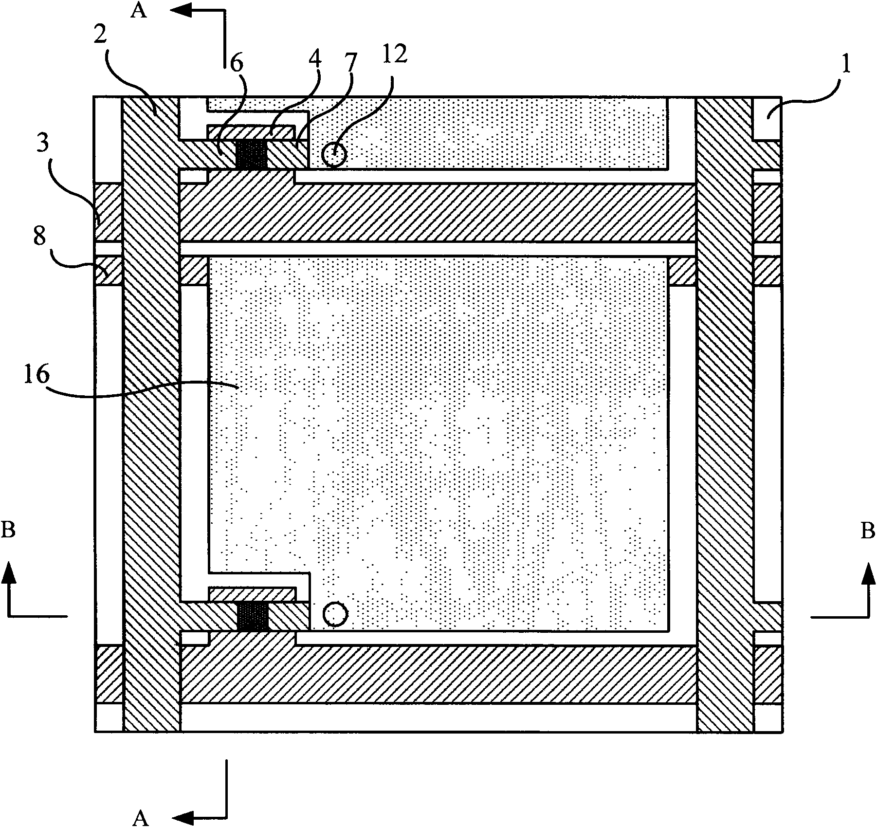
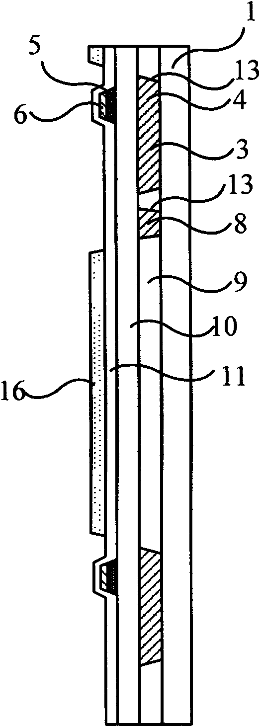
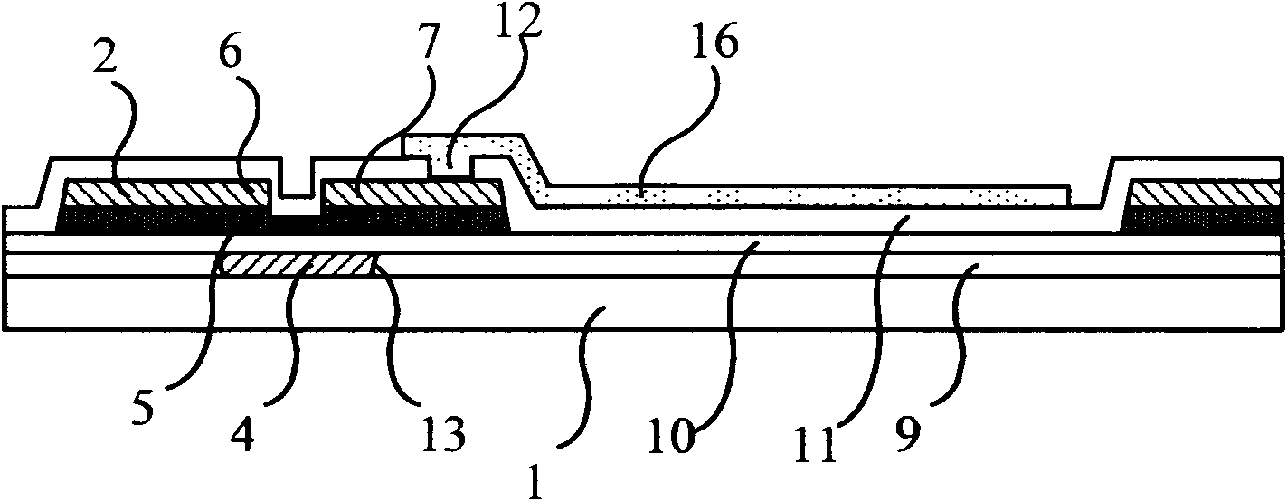
[0029] figure 1 It is a schematic diagram of a partial top view structure of a liquid crystal display substrate provided in Embodiment 1 of the present invention, figure 2 for figure 1 The schematic diagram of the cross-sectional structure in the A-A direction, image 3 for figure 1 A schematic diagram of the cross-sectional structure along the B-B direction in . The liquid crystal display substrate of this embodiment may specifically be an array substrate, including a base substrate 1 on which data lines 2 and gate scanning lines 3 crossing vertically and vertically are formed, surrounding a plurality of array substrates forming a matrix. pixel unit. Each pixel unit is provided with a TFT switch, and the TFT switch includes a gate electrode 4 , an active layer 5 , a source electrode 6 and a drain electrode 7 . The gate electrode 4 is connected to the gate scanning line 3, and is generally formed at the same time as the gate scanning line 3; the source electrode 6 is con...

Embodiment 2

[0038] Figure 4 The schematic diagram of the partial cross-sectional structure of the liquid crystal display substrate provided by Embodiment 2 of the present invention is different from Embodiment 1 in that the groove formed on the substrate insulating layer 9 also includes a second groove 14 formed on the gate insulating layer 10 The data line 2 , the source electrode 6 and the drain electrode 7 are formed in the second trench 14 . The top view structure of the liquid crystal display substrate in this embodiment can be found in figure 1 as shown, Figure 4 can be along figure 1 The schematic diagram of cutting the liquid crystal display substrate of this embodiment by the B-B line in the present embodiment, Figure 5 It is a partial top view structural schematic diagram of the substrate insulating layer 9 in the liquid crystal display substrate provided by Embodiment 2 of the present invention. The first groove 13 and the second groove 14 may be through grooves with equ...

Embodiment 3

[0043] Figure 6 It is a schematic diagram of a partial cross-sectional structure of a liquid crystal display substrate provided in Embodiment 3 of the present invention, Figure 7 It is a schematic diagram of a partial top view structure of the gate insulating layer 10 in the liquid crystal display substrate provided by Embodiment 3 of the present invention. In this embodiment, the insulating layer between the data line 2, the source electrode 6 and the drain electrode 7 and the gate scanning line 3, the gate electrode 4 and the common electrode line 8 is a gate insulating layer 10, and the insulating layer formed on the gate insulating layer 10 The trenches include a third trench 15 in which at least one or more of the data line 2 , the source electrode 6 and the drain electrode 7 are formed. The depth of the third trench 15 is smaller than the thickness of the gate insulating layer 10 , so as to avoid contact and conduction with the gate scanning line 3 under the gate insu...


PUM

PropertyMeasurementUnit
thicknessaaaaaaaaaa

Abstract

The invention relates to a liquid crystal display substrate and a manufacturing method thereof. The liquid crystal display substrate comprises a substrate; patterns of various conductive structures are formed on the substrate; and the conductive structures are mutually spaced or insulated through an insulating layer, wherein trenches are formed on the insulating layer with the conductive structures, and the patterns of the conductive structures are at least partially formed in the trenches. By adopting a technical means of forming the conductive structures in the trenches of the insulating layer, the height difference of the conductive structures on the surface of the insulating layer below the conductive structures is reduced, so that the limitation for the thickness of the conductive structures is reduced.

Description

technical field [0001] Embodiments of the present invention relate to liquid crystal display technology, and in particular to a liquid crystal display substrate and a manufacturing method thereof. Background technique [0002] Thin Film Transistor-Liquid Crystal Display (hereinafter referred to as TFT-LCD) has the characteristics of small size, low power consumption, and no radiation, and occupies a dominant position in the current flat panel display market. [0003] TFT-LCD usually includes two liquid crystal display substrates arranged in a cell, generally an array substrate and a color filter substrate in a cell, and liquid crystal is filled between them. The array substrate generally includes a base substrate on which data lines and gate scanning lines intersecting horizontally and vertically are formed, surrounding a plurality of pixel units forming a matrix. Each pixel unit is provided with a TFT switch, and the TFT switch includes a gate electrode, an active layer, a...

Claims


Application Information

Patent Timeline
Patent Type & Authority Applications(China)
IPC IPC(8): G02F1/1362G02F1/1368G03F7/00H01L23/528H01L21/768
Inventor 孙冰
Owner BOE TECH GRP CO LTD
Why Eureka
Try Eureka