Flat FCB (Flip Chip Bonding) GaN-based LED (Light-Emitting Diode) chip structure

A LED chip, flip-chip welding technology, applied in electrical components, electrical solid devices, circuits, etc., can solve the problems of limited thermal conductive metal bumps, chip PN short circuit, etc., to achieve better heat dissipation effect

Active Publication Date: 2011-04-27
HUAWEI TEHCHNOLOGIES CO LTD
View PDF3 Cites 20 Cited by
  • Summary
  • Abstract
  • Description
  • Claims
  • Application Information

AI Technical Summary

Problems solved by technology

[0006] Aiming at the problem that the heat-conducting metal bumps in the flip-chip structure are limited, and the bumps are too large to easily cause the PN short circuit of the chip, the invention proposes a flat flip-chip GaN-based LED chip with good heat dissipation effect and flat metal pads structure

Method used


Image

  • Flat FCB (Flip Chip Bonding) GaN-based LED (Light-Emitting Diode) chip structure
  • Flat FCB (Flip Chip Bonding) GaN-based LED (Light-Emitting Diode) chip structure
  • Flat FCB (Flip Chip Bonding) GaN-based LED (Light-Emitting Diode) chip structure

Examples


Embodiment Construction

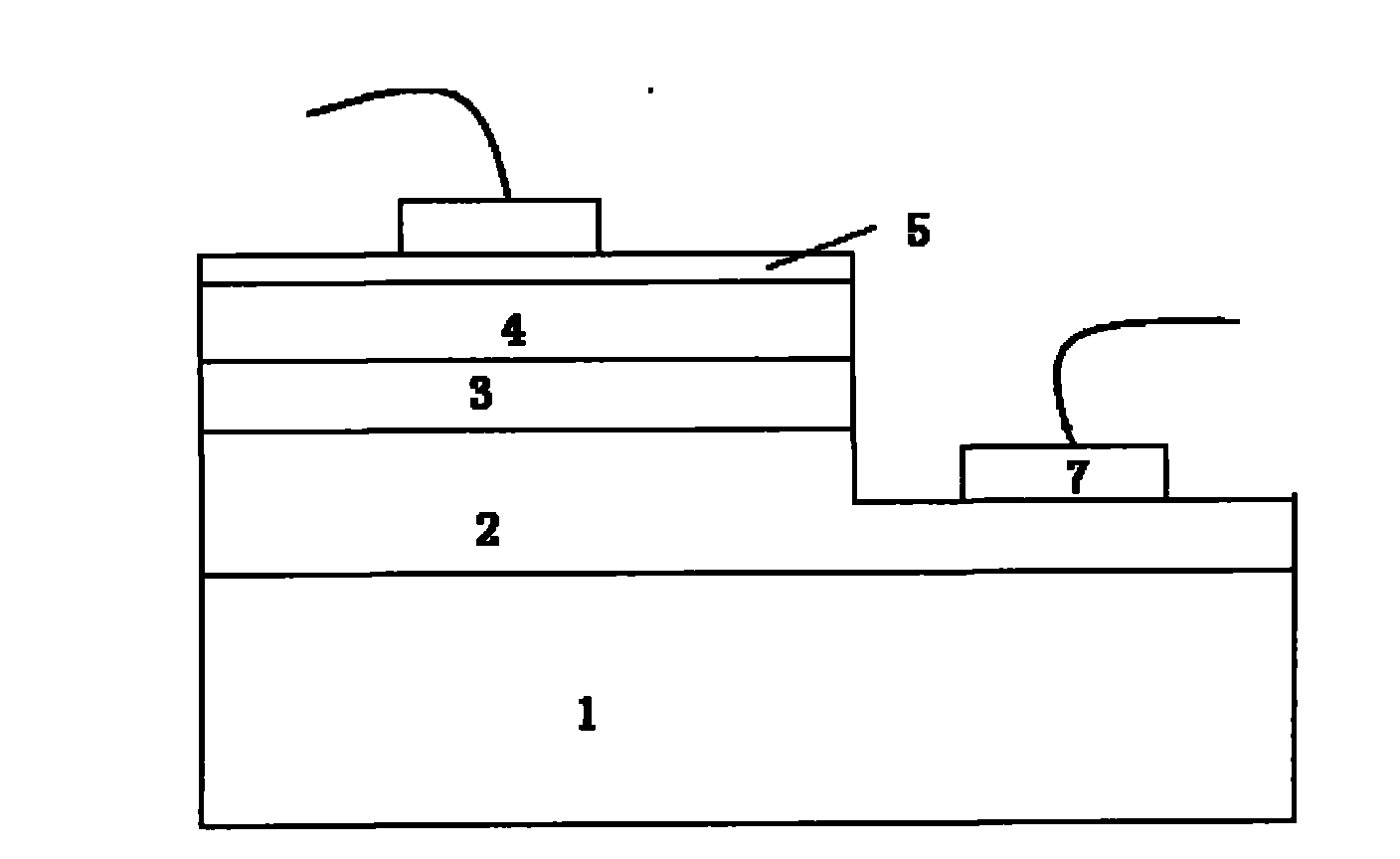
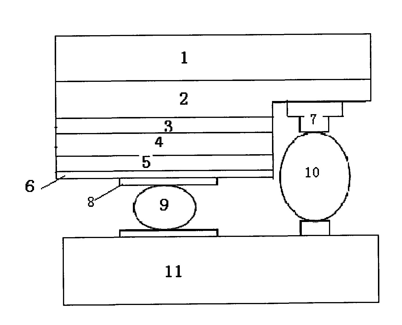
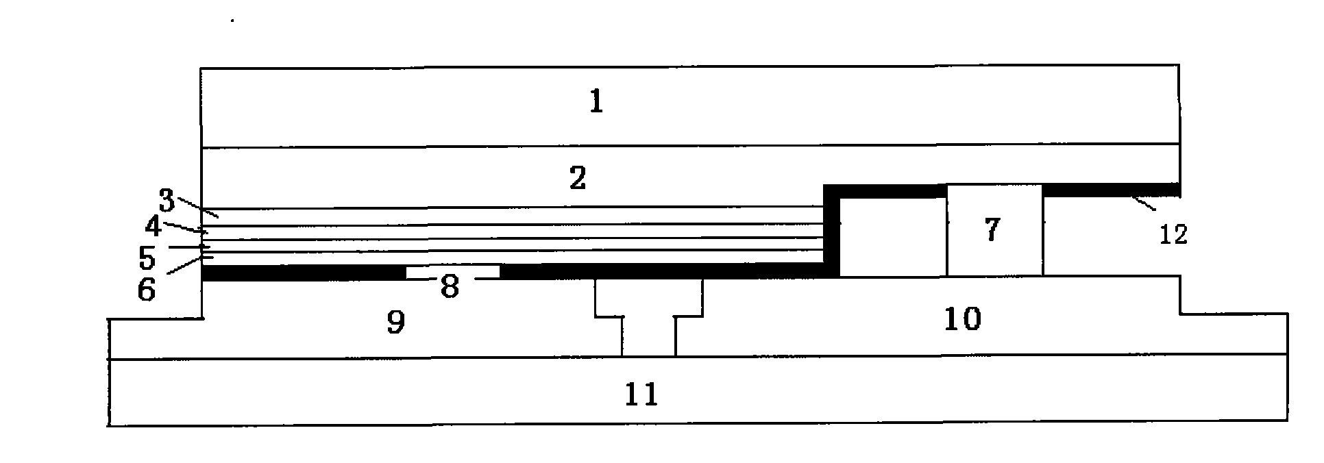
[0015] The structure of the flat panel flip-chip GaN-based LED of the present invention is in figure 2 Improvements are made based on the flip-chip structure shown, as image 3 and Figure 4 As shown, a step surface to the N-type GaN layer 4 is etched on the light reflection layer 6, an N electrode 7 is formed on the N-type GaN layer 4 of the step surface, and a P electrode 8 is formed on the light reflection layer 6, The outer ends of the N electrode 7 and the P electrode 8 are in the same horizontal plane. A layer of transparent insulating dielectric film 12 is plated on other areas except the P electrode pad and the N electrode pad on the surface where the P electrode pad and the N electrode pad are located. The outer end of the P electrode welding point is made with a P welding plate 9, and the outer end of the N electrode welding point is made with an N welding plate 10, and the P welding plate 9 and the N welding plate 10 are welded to the P electrode area and the N o...


PUM


Abstract

The invention provides a flat FCB (Flip Chip Bonding) GaN-based LED (Light-Emitting Diode) chip structure comprising a substrate. An N-type GaN layer, a QW (Quantum Well) active area, a P-type GaN layer, a current extension level and a light-reflecting layer are sequentially arranged below the substrate from top to bottom, a stepped surface to the N-type GaN layer is etched on the light-reflecting layer, an N electrode is made on the N-type GaN layer of the stepped surface, a P electrode is made on the light-reflecting layer and arranged on the same plane with the outer end of the P electrode, a transparent insulated medium film is coated on the plane of the P electrode bonding pad and the N electrode bonding pad except the regions of P electrode bonding pad and the N electrode bonding pad, a P bonding board is made at the outer end of the P electrode bonding spot, an N bonding board is made at the outer end of the bonding point of the N electrode, and the P bonding board and the N bonding board are bonded on a P electrode area and an N electrode area of a conductive Si or SiC substrate by cocrystallization or alloy. The insulated medium film is coated outside the PN bonding pads to prevent PN from being subjected to short circuits and a limit N-area electrode conductive flat is spliced to the P area desk.

Description

technical field [0001] The invention relates to a GaN-based blue LED (light-emitting diode) structure, which belongs to the technical field of light-emitting diode structures. Background technique [0002] The structure of a traditional sapphire substrate GaN-based LED (light-emitting diode) chip is as follows: figure 1 As shown, an N-type GaN layer 2, a quantum well QW active region 3, a P-type GaN layer 4, and a current spreading layer 5 are sequentially arranged on the substrate 1 from bottom to top, and an N electrode is arranged on the N-type GaN layer 2. 7. The electrodes are just located on the light-emitting surface of the chip. In this structure, a small portion of the P-type GaN layer 4 and the "light-emitting" layer is etched in order to make electrical contact with the underlying N-type GaN layer 2 . Light is extracted from the upper P-type GaN layer 4 . The limited electrical conductivity of the P-type GaN layer 4 requires a current diffusion layer 5 to be d...

Claims


Application Information

Patent Timeline
Patent Type & Authority Applications(China)
IPC IPC(8): H01L33/62H01L33/44H01L33/64
CPCH01L2224/14H01L2224/49107
Inventor 沈燕徐现刚徐化勇郑鹏
Owner HUAWEI TEHCHNOLOGIES CO LTD
Why Eureka
Try Eureka