Analog simulation method for RFID tag circuit

A technology of RFID tag simulation and simulation, which is applied in the field of simulation simulation of RFID tag circuits, and can solve problems such as not being completely identical and impedance not changing

Active Publication Date: 2012-09-05
SHANGHAI HUAHONG GRACE SEMICON MFG CORP
View PDF4 Cites 0 Cited by
  • Summary
  • Abstract
  • Description
  • Claims
  • Application Information

AI Technical Summary

Problems solved by technology

The disadvantage of the existing simulation method is that the loaded signal source is constant and its impedance does not change, such as Figure 2, the signal is a perfect sine wave, which is inconsistent with the waveform formed by the impedance changing at both ends of the antenna during the actual working process, and the actual chip The real physical environment is not exactly the same, and the designed chip needs to be taped out many times to be consistent with the data in the actual test environment.

Method used


Image

  • Analog simulation method for RFID tag circuit
  • Analog simulation method for RFID tag circuit
  • Analog simulation method for RFID tag circuit

Examples


Embodiment Construction

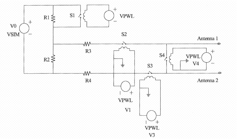
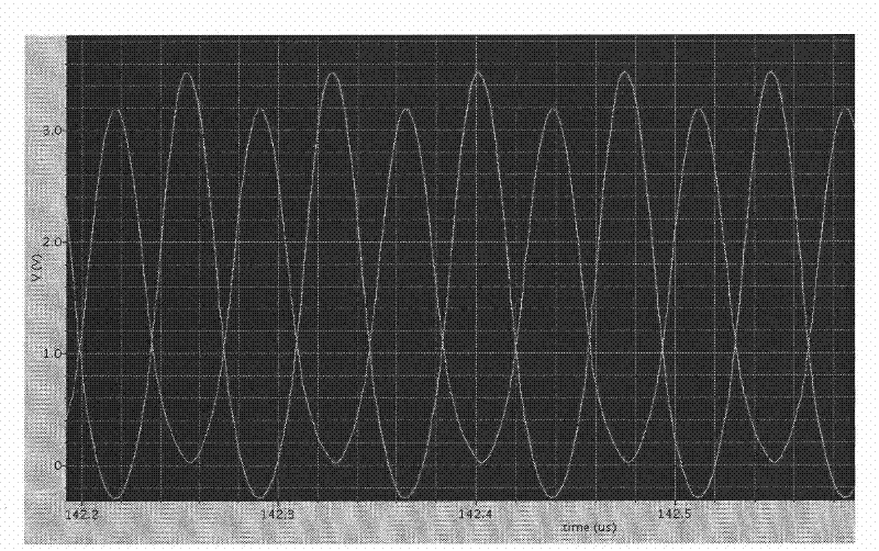
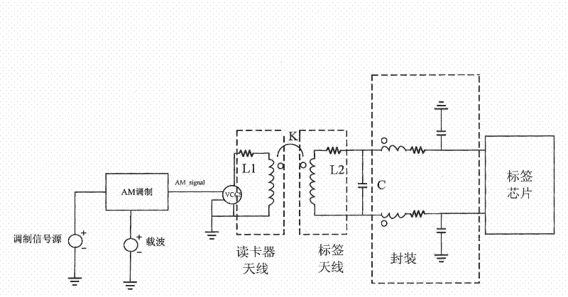
[0013] The invention discloses a simulation simulation method of an RFID tag circuit. The model of the RFID tag circuit completes various simulation operations by receiving a signal through an antenna. The invention uses a model of an amplitude modulator to simulate a modulated signal transmitted by a card reader. Carrier and its energy, and the signal is coupled from the amplitude modulator to the antenna of the RFID tag circuit through a mutual inductance coefficient to simulate the actual field strength.

[0014] The working principle of the RFID tag specified in the ISO14443 protocol is to use the inductive magnetic coupling of the reader and the tag antenna for data communication. As a passive tag, the DC power supply of the tag can be obtained from the reader through the inductive magnetic coupling. The reader generates a strong high-frequency electromagnetic field, which penetrates the cross section of the antenna and the space around the coil, because the wavelength in the...


PUM


Abstract

The invention discloses an analog simulation method for a radio frequency identification (RFID) tag circuit. The method comprises that: a model of the RFID tag circuit receives a signal through an antenna to complete various simulation operations, a model of an amplitude modulator simulates a carrier of a modulation signal transmitted by a card reader and energy thereof, and the signal is coupled to the antenna of the RFID tag circuit from the amplitude modulator through a mutual inductance coefficient so as to simulate the magnitude of actual field intensity. By simulating the card reader to transmit the signal through the amplitude modulator and coupling the signal to a chip of the RFID tag circuit through the mutual inductance coefficient, a real working environment of the RFID tag circuit is simulated, and the RFID tag circuit is accurately simulated.

Description

technical field [0001] The invention relates to a simulation method of a semiconductor circuit, in particular to a simulation method of an RFID tag circuit. Background technique [0002] The existing RFID system consists of an HF card reader that emits a 13.56MHz signal, a tag, and an antenna. The actual transmitted carrier wave with a modulated signal is coupled with the antenna of the tag through the physical space, and the tag chip passes through its own The antenna and the internal capacitor resonate, the passive tag chip takes out energy through the rectifier as the power supply of the whole chip, and the demodulator of the tag chip demodulates and outputs the signal sent by the card reader. The tag chip signal is transmitted by changing the load on the antenna, so that the resonance amplitude of the tag antenna changes, and through the coupling with the card reader antenna, the amplitude of the card reader antenna also changes. The signal amplification circuit and the...

Claims


Application Information

Patent Timeline
Patent Type & Authority Patents(China)
IPC IPC(8): G06F17/50G06K19/07
Inventor 朱红卫
Owner SHANGHAI HUAHONG GRACE SEMICON MFG CORP
Why Eureka
Try Eureka