Method for forming contact hole

A technology of contact hole and hard mask layer, which is applied in the field of contact hole formation, and can solve the problems of small dielectric layer thickness, easy breakdown or leakage, short circuit, etc.

Inactive Publication Date: 2011-05-11
SEMICON MFG INT (SHANGHAI) CORP
View PDF3 Cites 14 Cited by
  • Summary
  • Abstract
  • Description
  • Claims
  • Application Information

AI Technical Summary

Problems solved by technology

[0009] As mentioned above, during the process of plasma etching, the wafer has been exposed to the plasma environment containing high-density reactive ions and high-energy bombardment ions for a long time. The etching will cause the bombardment ions to be distributed unevenly on the wafer surface, and the top of the contact hole in some parts will be over-etched, which will increase the opening width of the top of the contact hole, and eventually lead to the deposition of metal materials in the contact hole to form an interconnection structure. As the thickness of the dielectric layer between adjacent interconnection structures becomes smaller, breakdown or short circuit occurs between adjacent interconnection structures
[0010] Reference attached Image 6 As shown, it is a top view of the contact hole array. The depth of the contact hole in the figure is greater than 3um, and the etching time for etching the insulating dielectric layer to form the contact hole is greater than 500 seconds. It can be seen from the figure that the adjacent two contact holes The distance D1 between them is smaller than the distance D2 between the other two adjacent contact holes. For two adjacent contact holes with a distance of D1, breakdown or leakage is more likely to occur.

Method used


Image

  • Method for forming contact hole
  • Method for forming contact hole
  • Method for forming contact hole

Examples


Embodiment Construction

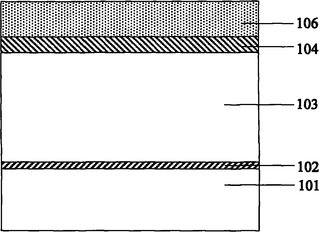
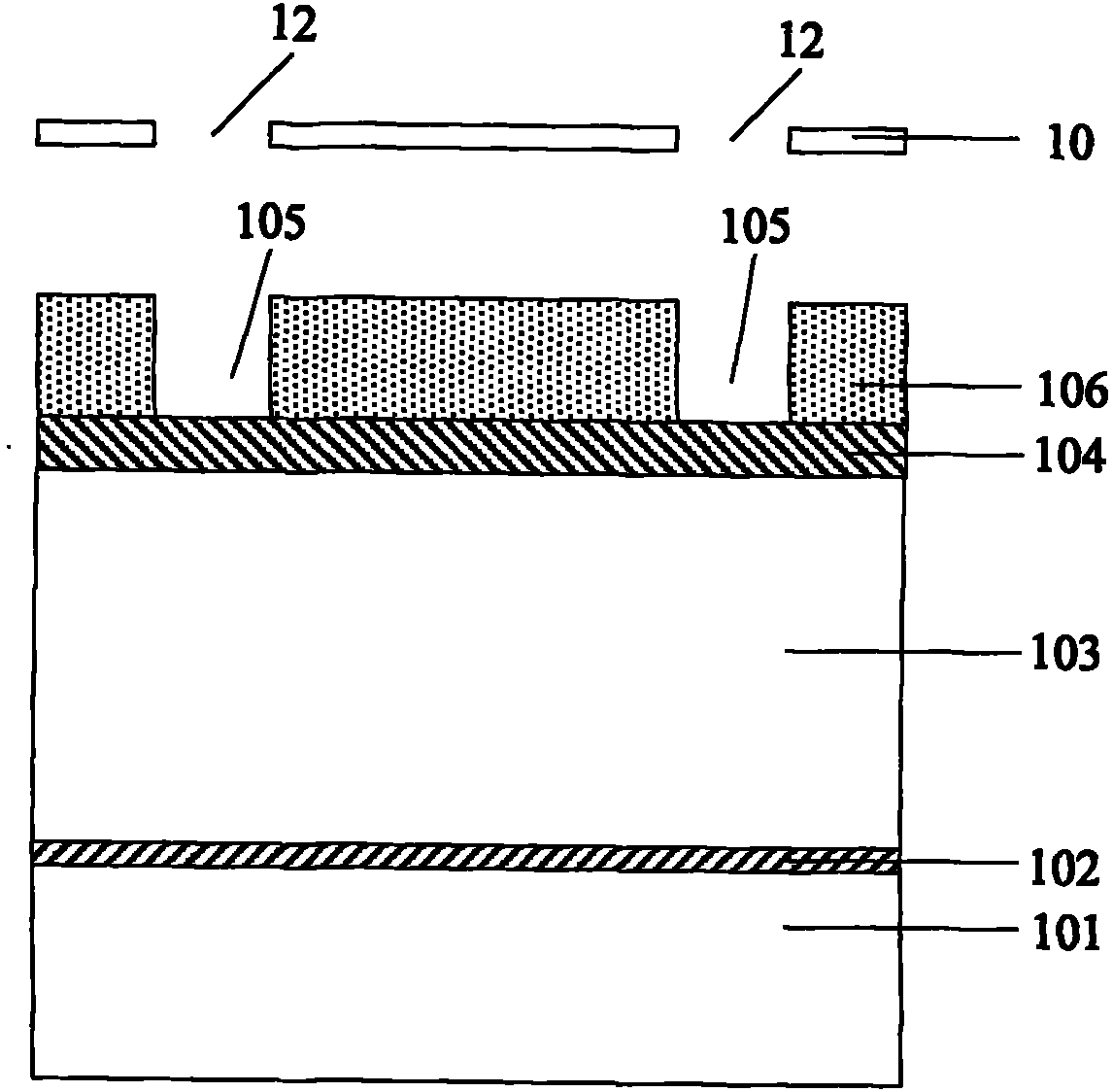
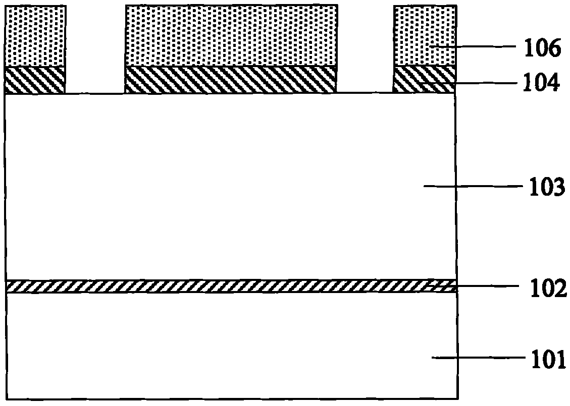
[0020] In the following description, numerous specific details are set forth in order to provide a thorough understanding of the present invention. However, the present invention can be implemented in many other ways different from those described here, and those skilled in the art can make similar extensions without violating the connotation of the present invention, so the present invention is not limited by the specific embodiments disclosed below.

[0021] Secondly, the present invention is described in detail using schematic diagrams. When describing the embodiments of the present invention in detail, for the convenience of explanation, the cross-sectional view showing the device structure will not be partially enlarged according to the general scale, and the schematic diagram is only an example, and it should not be limited here. The protection scope of the present invention. In addition, the three-dimensional space dimensions of length, width and depth should be include...


PUM


Abstract

The invention discloses a method for forming a contact hole, which comprises the following steps of: sequentially forming an insulating medium layer, a hard mask layer and a photoresist layer on a semiconductor substrate; forming the graph of a contact hole opening on the photoresist layer; by taking the photoresist layer as a mask, etching the hard mask layer along the graph of the contact hole opening so as to form the contact hole opening; removing the photoresist layer; by taking the hard mask layer as the mask, etching the insulating medium layer to a certain depth along the contact holeopening by a plasma etching process, wherein the depth is one third to three fourths of the depth of a target contact hole; determining the type of charged ions accumulated on the surface of the hardmask layer, and introducing plasmas of which the type is opposite to that of the charged ions into a reaction chamber until the charged ions are neutralized; and by taking the hard mask layer as the mask, continuing to etch the insulating medium layer until the semiconductor substrate is exposed so as to form the target contact hole. The contact holes with uniform opening width can be formed by the method.

Description

technical field [0001] The invention relates to the field of manufacturing semiconductor devices, in particular to a method for forming a contact hole. Background technique [0002] With the rapid development of ULSI (Ultra Large Scale Integration), the manufacturing process of integrated circuits has become more and more complex and sophisticated. In order to improve the integration level and reduce the manufacturing cost, the key dimensions of the components are getting smaller and the number of components per unit area of ​​the chip is increasing. The vertical space further increases the integration density of the device. Metal material needs to be deposited in the contact holes between the wirings of each layer for electrical connection. [0003] As the critical dimension of the component becomes smaller, the critical dimension of the contact hole becomes smaller and smaller. At the same time, the depth of the contact hole becomes larger (the aspect ratio of the contac...

Claims


Application Information

Patent Timeline
Patent Type & Authority Applications(China)
IPC IPC(8): H01L21/768
Inventor 邹立罗飞
Owner SEMICON MFG INT (SHANGHAI) CORP
Why Eureka
Try Eureka