Device for testing life of semiconductor laser

A technology of life testing and laser, which is applied in the direction of optical instrument testing, measuring device, machine/structural component testing, etc., can solve the problem of difficulty in ensuring test accuracy and stability, low power range of laser test, and difficulty in reflecting the real life of laser. Process and other issues to achieve multi-functionality and improve test efficiency

Active Publication Date: 2011-05-18
FOCUSLIGHT TECH
View PDF4 Cites 48 Cited by
  • Summary
  • Abstract
  • Description
  • Claims
  • Application Information

AI Technical Summary

Problems solved by technology

[0008] However, the existing laser life test systems generally have a low test power range for lasers, and most of the laser life test systems developed in China focus on manual measurement or theoretical derivation
This method is difficult to guarantee the accuracy and stability of the test, especially for high-power laser testing, the data is difficult to reflect the real life of the laser working process

Method used


Image

  • Device for testing life of semiconductor laser
  • Device for testing life of semiconductor laser
  • Device for testing life of semiconductor laser

Examples


Embodiment Construction

[0030] The present invention is described in further detail below in conjunction with accompanying drawing:

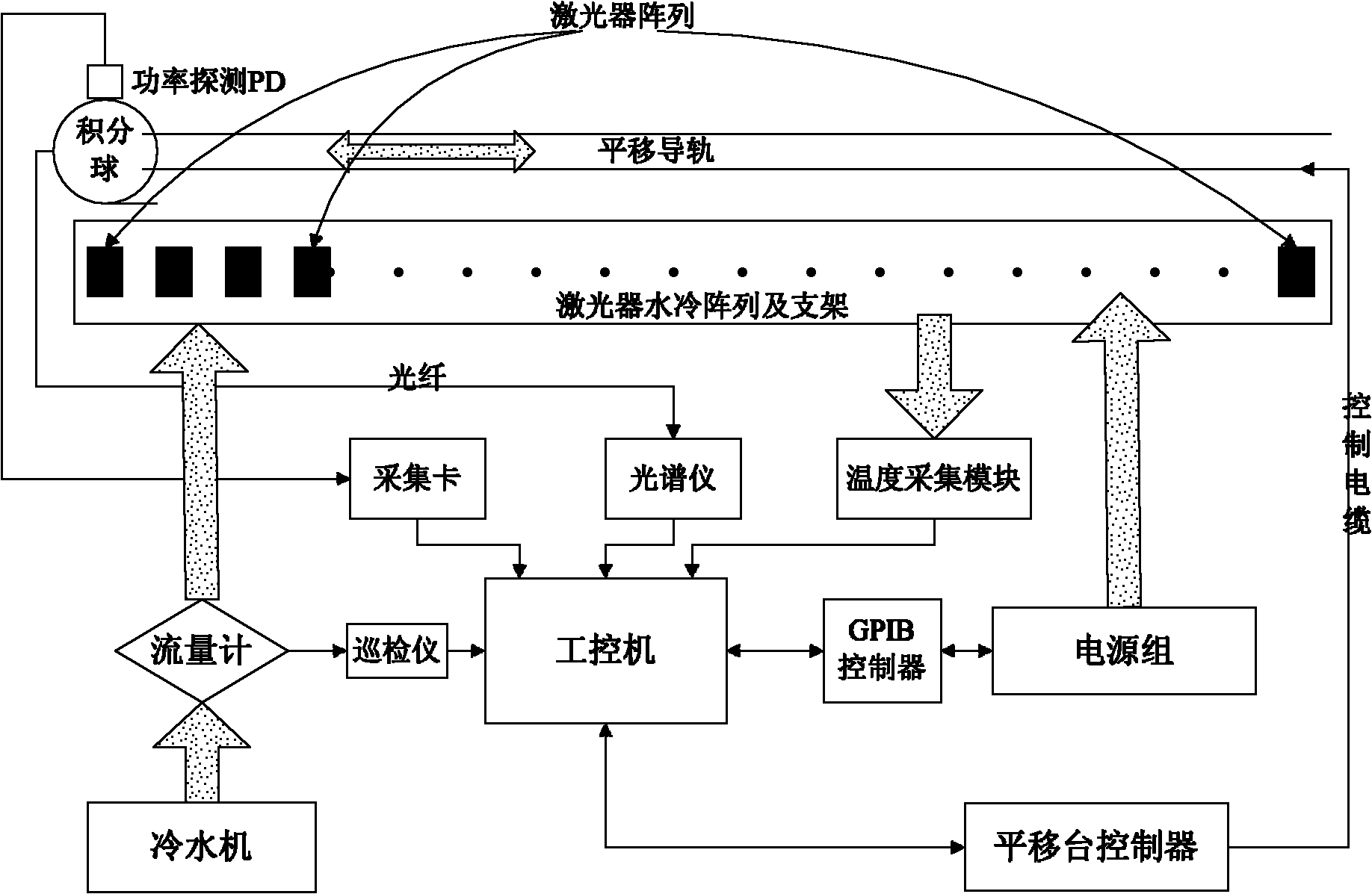
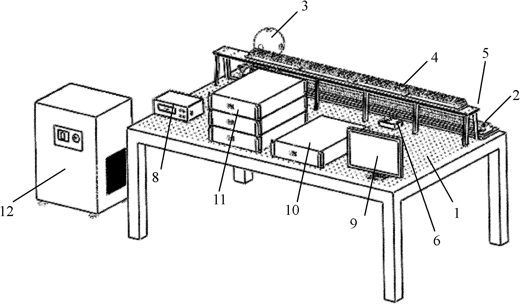
[0031] see figure 1 with figure 2 , the semiconductor laser life testing device of the present invention includes an optical platform 1 and an industrial computer 10 arranged on the optical platform 1 . The optical platform 1 is also provided with parallel guide rails 2 and a laser water-cooled array 4 , and the laser water-cooled array 4 is fixed on the optical platform 1 through a bracket 5 . The laser water cooling array 4 and the parallel guide rails 2 are parallel to each other. An electric translation platform is arranged on the parallel guide rail 2, and an integrating sphere 3 and a power detection PD are fixed on the electric translation platform. The integrating sphere 3 is connected to a spectrometer 6 through an optical fiber, and the spectrometer 6 is connected to the industrial computer 10; Connect with industrial computer 10. A temperature acquisiti...


PUM


Abstract

The invention discloses a device for testing life of a semiconductor laser, comprising an optical platform, wherein the optical platform is provided with parallel guide rails and a laser water cooling array; the parallel guide rails are provided with electric translation tables; an integrating sphere and a PD (Power Detector) are fixed on the electric translation tables; the integrating sphere isconnected with a spectrograph through an optical fiber; the spectrograph is connected to an industrial personal computer; the PD is connected with the industrial personal computer through a collecting card; a temperature collecting module is arranged at the side of the laser water cooling array and connected with the industrial personal computer; the electric translation tables are connected witha translation table controller through controlling a cable; and the translation table controller is connected to the industrial personal computer. By the system, automatic parameter tests can be carried out on laser products with different packaging types, powers and numbers. The power and the spectral information of the laser products are automatically collected and recorded in the processing ofworking, the report printing data can be automatically carried out to form a test report, and therefore, the basis for failure analysis and research of the laser products is provided.

Description

technical field [0001] The invention belongs to the technical field of laser testing, and relates to a laser testing device, in particular to a device for testing the life of a high-power semiconductor laser. Background technique [0002] High-power semiconductor lasers are widely used in communication, military, medical and many other fields. As an important index to measure laser products, its reliability has been paid more and more attention by people. This is mainly due to: [0003] (1) Through the reliability research of semiconductor lasers, the failure mechanism of semiconductor lasers can be accurately judged. [0004] (2) Test the actual working life time of the semiconductor laser. [0005] (3) Provide a basis for the aging research of semiconductor lasers. [0006] (4) To improve device design and process technology to improve the reliability of semiconductor lasers. [0007] However, since the life test of high-power semiconductor lasers often requires regul...

Claims


Application Information

Patent Timeline
Patent Type & Authority Applications(China)
IPC IPC(8): G01M11/00G01J1/00G01J3/28
Inventor 刘兴胜代华斌张彦鑫李锋吴迪
Owner FOCUSLIGHT TECH
Why Eureka
Try Eureka