Boron-aluminum process for high-power transistor chip

A high-power transistor and diffusion process technology, which is applied in semiconductor/solid-state device manufacturing, electrical components, circuits, etc., can solve the problems of product performance impact, slow diffusion rate, small PN junction space, etc., and achieve high reliability requirements, anti-corrosion The effect of improving the burning ability and stabilizing the magnification

Active Publication Date: 2011-05-25
西安卫光科技有限公司
View PDF2 Cites 9 Cited by
  • Summary
  • Abstract
  • Description
  • Claims
  • Application Information

AI Technical Summary

Problems solved by technology

This diffusion process has the following disadvantages: 1. The diffusion rate is slow; 2. The diffusion depth is limited, usually 40um to 50um. The limited diffusion depth makes the formed PN junction space small, and the performance of the product is also affected.

Method used


Image

  • Boron-aluminum process for high-power transistor chip

Examples


Embodiment 1

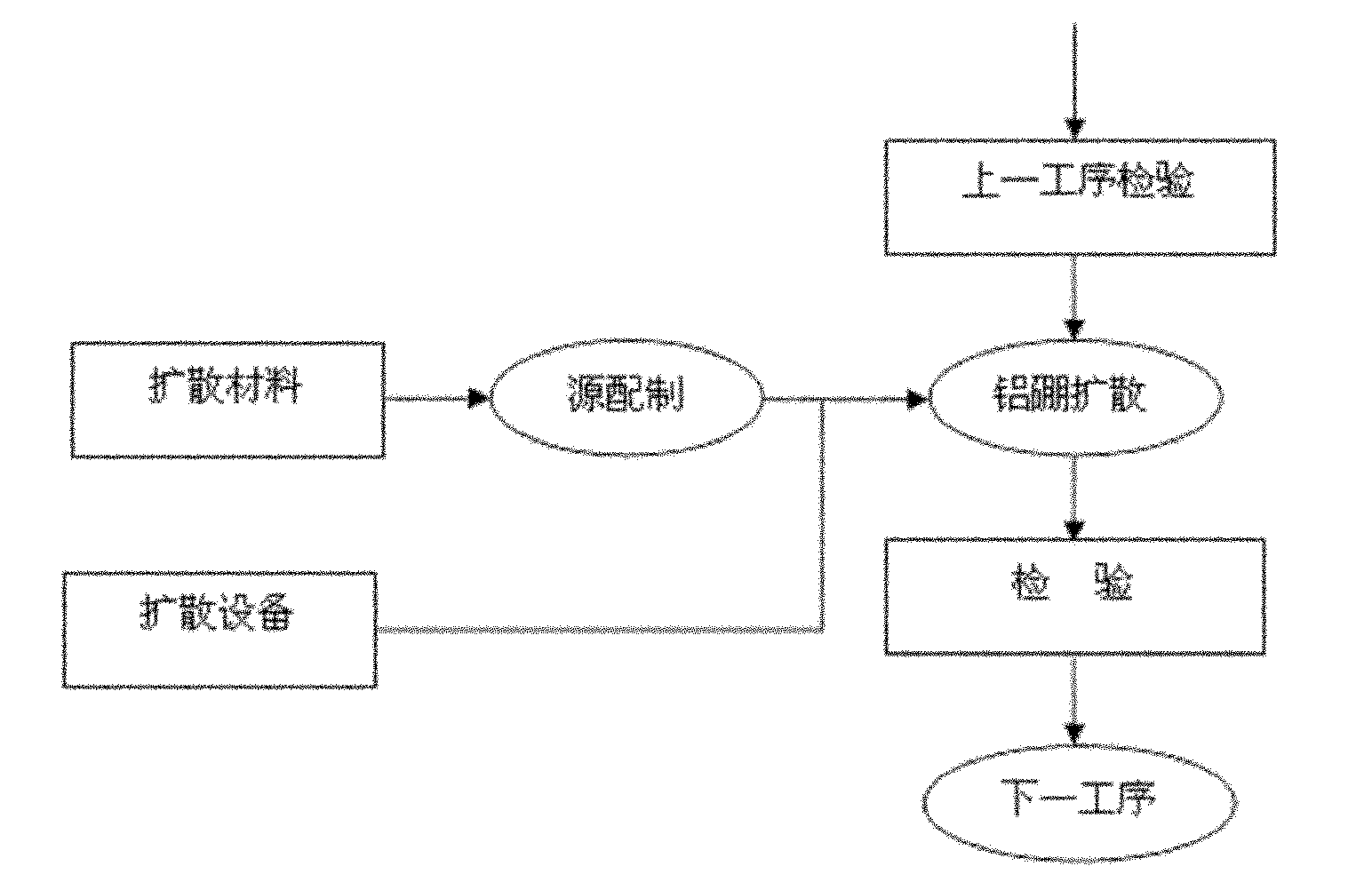
[0035] see figure 1 Shown, technique of the present invention comprises the following steps:

[0036] 1. Preparation of source solution: 40 grams of pure aluminum nitrate, 1.5 grams of diboron trioxide dissolved in 500ml of ethanol (electronic pure) and ultrasonicated for 4 hours to ensure full dissolution;

[0037] 2. Silicon wafer cleaning: Put the silicon wafer into deionized water and ultrasonically remove sand until the ionized water is clear; then put the sand-removed silicon wafer into a quartz beaker, add No. 1 standard cleaning solution (NH 4 OH / H 2 o 2 / H 2 O is mixed according to the ratio of 1:1:5 to 1:2:7), heated to boiling, and kept for 5 minutes, then removed and washed with deionized water;

[0038] 3. Drying of silicon wafers: dehydrate the cleaned silicon wafers in step 2 with absolute ethanol, and dry them in an oven at 120±3°C;

[0039] 4. Coat the surface of the silicon wafer dried in step 3 with the source solution prepared in step 1; suck the sourc...

Embodiment 2

[0041] Present embodiment technology comprises the following steps:

[0042] 1. Preparation of source solution: 40 grams of pure aluminum nitrate, 2 grams of diboron trioxide dissolved in 500ml of ethanol (electronic pure) and ultrasonicated for 4 hours to ensure full dissolution;

[0043] 2. Silicon wafer cleaning: Put the silicon wafer into deionized water to remove sand by ultrasonic until the ionized water is clear; then put the sand-removed silicon wafer into a quartz beaker, add No. 1 standard cleaning solution, heat to boiling, and keep the time 8 minutes, then remove and wash with deionized water;

[0044] 3. Drying of silicon wafers: dehydrate the cleaned silicon wafers in step 2 with absolute ethanol, and dry them in an oven at 120±3°C;

[0045] 4. Coat the surface of the silicon wafer dried in step 3 with the source solution prepared in step 1; suck the source with a dropper, and apply it evenly on the grinding surface. After the source solution is slightly dry, ap...

Embodiment 3

[0047] Present embodiment technology comprises the following steps:

[0048] 1. Preparation of source solution: 40 grams of pure aluminum nitrate, 2.5 grams of diboron trioxide dissolved in 500ml of ethanol (electronic pure) and ultrasonicated for 4 hours to ensure full dissolution;

[0049] 2. Silicon wafer cleaning: Put the silicon wafer into deionized water to remove sand by ultrasonic until the ionized water is clear; then put the sand-removed silicon wafer into a quartz beaker, add No. 1 standard cleaning solution, heat to boiling, and keep the time 10 minutes, then remove and wash with deionized water;

[0050] 3. Drying of silicon wafers: dehydrate the cleaned silicon wafers in step 2 with absolute ethanol, and dry them in an oven at 120±3°C;

[0051] 4. Coat the surface of the silicon wafer dried in step 3 with the source solution prepared in step 1; suck the source with a dropper, and apply it evenly on the grinding surface. After the source solution is slightly dry,...


PUM


Abstract

The invention relates to a boron-aluminum diffusion process for a high-power transistor chip. The process comprises the following steps of: 1) preparing source solution, namely dissolving a grams of pure aluminum nitrate, b grams of diboron trioxide into c ml of ethanol; 2) washing a silicon chip; 3) drying the silicon chip; and 4) uniformly coating the source solution prepared in step 1) on the surface of the silicon chip dried in the step 3), placing the silicon chip into a diffusion furnace, rising the temperature to 1,260+ / -1 DEG C and keeping the constant temperature for 8 to 10 hours, wherein a:b:c=40:(1.5-2.5):500. In the boron-aluminum diffusion process for the high-power transistor chip, a process method for simultaneously diffusing the boron and the aluminum is adopted; the diffusion depth of the boron can reach 100 to 110 mu m by utilizing high diffusion rate of the aluminum and high surface concentration of the boron at a high temperature, so that the burnback resistance of a product is improved greatly; an amplification factor is more stable; and the product is used in special fields with harsh environment and high reliability requirement.

Description

【Technical field】 [0001] The invention relates to the technical field of semiconductor element preparation, in particular to a processing technology of a high-power transistor chip. 【Background technique】 [0002] Transistor is an important semiconductor component with a wide range of applications. As the core component of the transistor, the processing of the transistor chip usually adopts the method of doping the silicon wafer to form a PN junction, that is, the boron element is diffused into the silicon wafer at high temperature to form a PN junction. This diffusion process has the following disadvantages: 1. The diffusion rate is slow; 2. The diffusion depth is limited, usually 40um-50um. The limited diffusion depth makes the formed PN junction space small, and the performance of the product is also affected. 【Content of invention】 [0003] The object of the present invention is to provide a boron-aluminum diffusion process for a high-power transistor chip. The boron ...

Claims


Application Information

Patent Timeline
Patent Type & Authority Applications(China)
IPC IPC(8): H01L21/228
Inventor 高勇
Owner 西安卫光科技有限公司
Why Eureka
Try Eureka