Box-method boron microcrystalline glass source concentrated boron diffusion method

A glass-ceramic and borosilicate glass technology, applied in electrical components, semiconductor/solid-state device manufacturing, circuits, etc., can solve the problems of high surface concentration, long process flow, affecting the series resistance parameters of products, etc.

Pending Publication Date: 2022-02-08
CHENGDU YAGUANG ELECTRONICS
View PDF0 Cites 0 Cited by
  • Summary
  • Abstract
  • Description
  • Claims
  • Application Information

AI Technical Summary

Problems solved by technology

[0005] However, the open-tube diffusion method has a long and complicated process flow, and the main diffusion used is limited surface source diffusion. When it is applied to the process of low-voltage PIN diodes, the junction depth can be controlled, but when impurities are redistributed (main diffusion) , the surface concentration is not as high as the box method concent

Method used


Image

  • Box-method boron microcrystalline glass source concentrated boron diffusion method
  • Box-method boron microcrystalline glass source concentrated boron diffusion method
  • Box-method boron microcrystalline glass source concentrated boron diffusion method

Examples


Embodiment

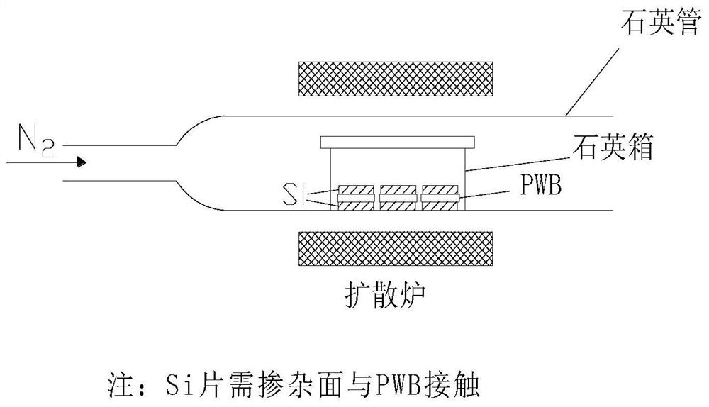
[0050] Box Fault Boron Crystalline Glass Source (PWB) Concentrated boron diffusion technology (constant surface source diffusion), similar to the diffusion of the closed tube, but no seal, different from A S Diffusion needs to be completely sealed.

[0051] The solid-state PWB is used to treat the boron source. Treatment steps: repeatedly wipe the boron source with acetone, then rush, heat, heat, cold ion water, and put it in the infrared light oven to dry the source surface, 30 min However, raise the diffusion furnace to 1100 ° C, and the diffusion furnace 2 The flow rate is 1 l / min, put the PWB source in the quartz boo boat in the quartz box, cover the quartz box, push into the constant temperature zone of the diffusion furnace, and bake over 24 hours or more.

[0052] Boxa Boron Microcrystalline Glass Source (PWB) Concentrated boron diffusion step: raise the diffusion furnace to 1100 ° C, pass N 2 1 l / min, the quartz box equipped with a boron source is pushed into the const...


PUM


Abstract

The invention provides a box-method boron microcrystalline glass source concentrated boron diffusion method which comprises the steps of S1) carrying out high-temperature pretreatment on boron microcrystalline glass to obtain pretreated boron microcrystalline glass; S2) stacking the pretreated boron microcrystalline glass and a silicon wafer to be subjected to diffusion treatment, and heating for diffusion treatment to obtain a treated silicon wafer, wherein the front surface of the silicon wafer to be subjected to diffusion treatment is in contact with the pretreated boron microcrystalline glass; and S3) removing borosilicate glass on the surface of the treated silicon wafer to obtain the silicon wafer subjected to boron diffusion treatment. Compared with the prior art, the PWB source is in direct contact with the Si wafer, so that a shallow junction can be formed while high surface concentration is realized; secondly, the upper surface and the lower surface of the PWB source can be in contact with the to-be-doped surfaces of the two layers of Si wafers respectively, so that the diffusion efficiency is improved; moreover, the method provided by the invention only uses one-step diffusion, does not need to take out the Si wafer midway for treatment, is simple in process and easy to operate, and avoids unnecessary pollution.

Description

Technical field [0001] The present invention belongs to the microwave semiconductor technology, and in particular, the present invention relates to a method of dip boron diffusion of boron microcrystalline glass sources. Background technique [0002] Microwave semiconductor diffusion process technology is divided into: constant surface source diffusion and defining surface source diffusion. Under ideal, when the constant surface source diffuses, the impurity concentration is distributed in the depth of the surface, the surface concentration is always constant, and the time is independent; the concentration of the diffusion impurities defining the surface source is Gaussian distribution, when the diffusion temperature is maintained When constant, as the diffusion time increases, the concentration of surface impurities continues to decrease, but the total amount of diffusion impurities remain unchanged. [0003] In terms of boron diffusion sources of p-type dopants, trimethylation,...

Claims


Application Information

Patent Timeline
IPC IPC(8): H01L21/225
CPCH01L21/2251
Inventor 杨青
Owner CHENGDU YAGUANG ELECTRONICS
Why Eureka
Try Eureka