

Forming method of N-channel metal oxide semiconductor (NMOS) transistor
A transistor and semiconductor technology, applied in semiconductor/solid-state device manufacturing, electrical components, circuits, etc., can solve the problems of device characteristic drift, fast rise of threshold voltage in channel region, uneven ion distribution in Vt implantation region, etc. Short channel effect, uniform ion distribution effect
- Summary
- Abstract
- Description
- Claims
- Application Information
AI Technical Summary
Problems solved by technology
Method used
Image

Examples
Embodiment Construction
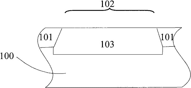
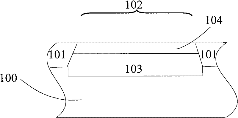
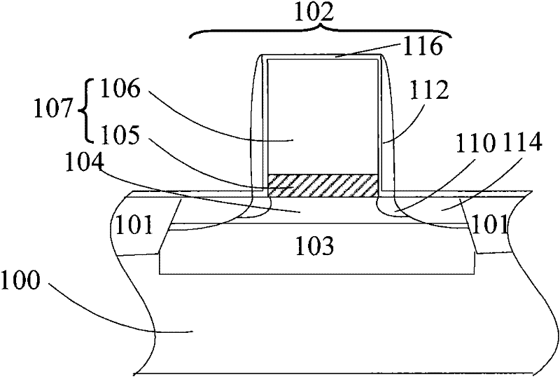
[0019] The specific implementation process of forming NMOS transistors in the present invention is as follows: Figure 4 As shown, step S1 is executed to provide a semiconductor substrate, and the semiconductor substrate is divided into an isolation region and an active region; step S2 is executed to form a doped well in the semiconductor substrate in the active region; step S3 is executed to form a doped well in the active region A gate dielectric layer and a gate are sequentially formed on the semiconductor substrate in the source region, and the gate dielectric layer and the gate form a gate structure; step S4 is performed to re-oxidize the gate structure; step S5 is performed to take the gate structure as Mask, implanting ions into the semiconductor substrate on both sides of the gate to form source / drain extension regions; performing step S6, forming Vt implantation regions in the semiconductor substrate after forming sidewalls on both sides of the gate structure; Step S7...
PUM
 Abstract
Description
Claims
Application Information