
Light emitting diode with sandwich-type current blocking structure

A technology of light-emitting diodes and current blocking, applied in circuits, electrical components, semiconductor devices, etc., can solve the problems of reducing the probability of light emission from the side and affecting the light-extraction efficiency of light-emitting diodes

Active Publication Date: 2011-05-25
XIAMEN SANAN OPTOELECTRONICS TECH CO LTD
View PDF1 Cites 18 Cited by
  • Summary
  • Abstract
  • Description
  • Claims
  • Application Information

AI Technical Summary

Problems solved by technology

Therefore, the gallium nitride-based light-emitting diodes with a current blocking structure produced according to the existing technology, because the current distribution is more concentrated in the local area near the center of the chip, resulting in a lower probability of side light emission, which ultimately affects the light extraction efficiency of the light-emitting diode.

Method used


Image

  • Light emitting diode with sandwich-type current blocking structure
  • Light emitting diode with sandwich-type current blocking structure
  • Light emitting diode with sandwich-type current blocking structure

Examples


Embodiment Construction

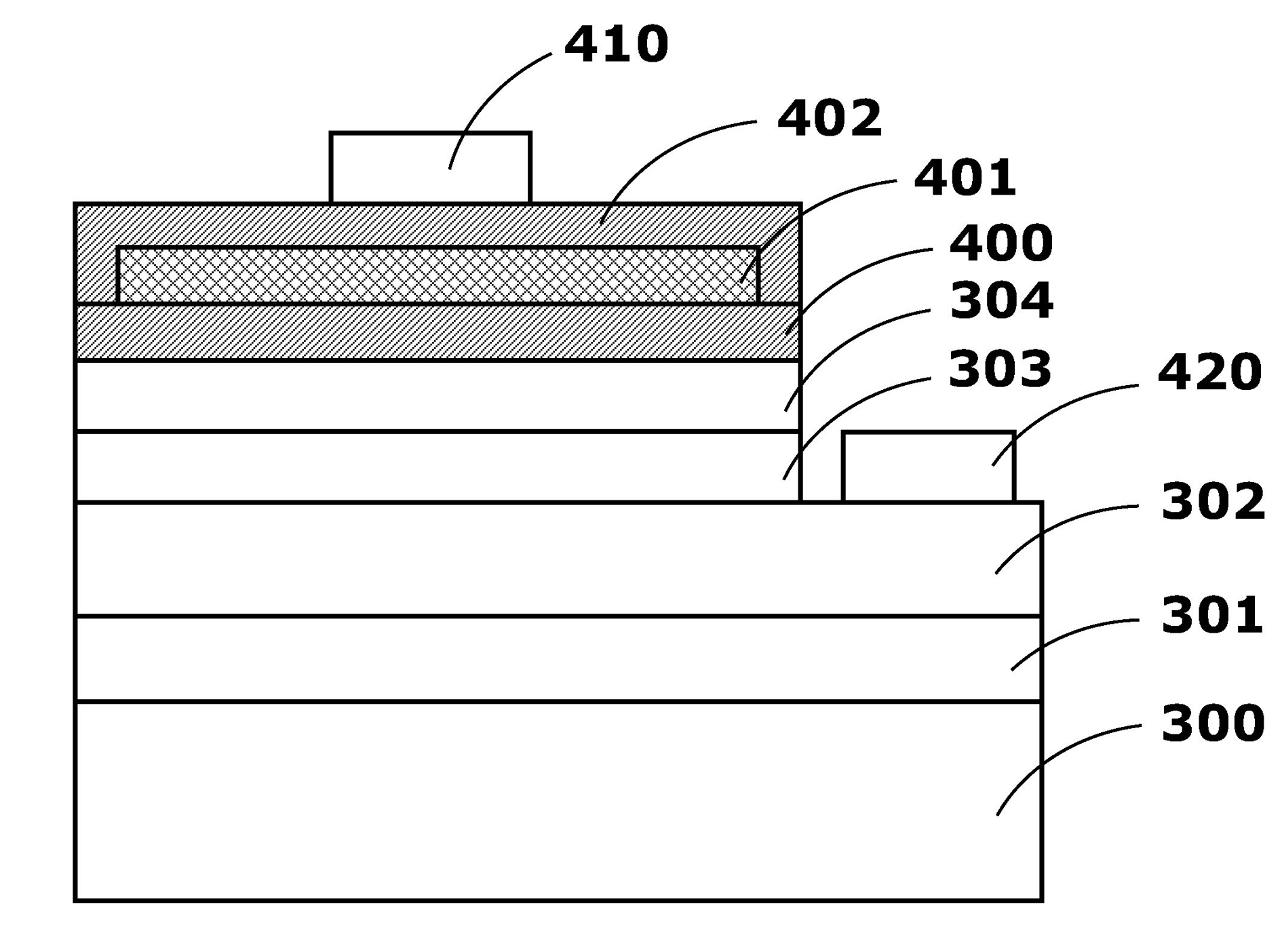
[0019] The present invention will be further described below in conjunction with Fig. 3, Fig. 4 and embodiments.

[0020] Such as image 3 A gallium nitride-based light-emitting diode structure with a sandwich current blocking structure is shown, which includes a sapphire substrate 300, a buffer layer 301, an n-GaN layer 302, a multi-quantum well active layer 303, and a p-GaN layer 304 , the first ITO layer 400, Si 3 N 4 layer 401 , second ITO layer 402 , p-electrode 410 and n-electrode 420 . Wherein, the lowest layer is the sapphire substrate 300; the buffer layer 301 is formed on the sapphire substrate 300; the n-GaN layer 302 is formed on the buffer layer 301; the multi-quantum well active layer 303 is formed on the n-GaN layer 302 The material is indium gallium nitride (InGaN); the p-GaN layer 304 is formed on the multi-quantum well active layer 303 ; the first ITO layer 400 is formed on the p-GaN layer 304 .

[0021] In the present invention, "the first ITO layer 40...


PUM


Abstract

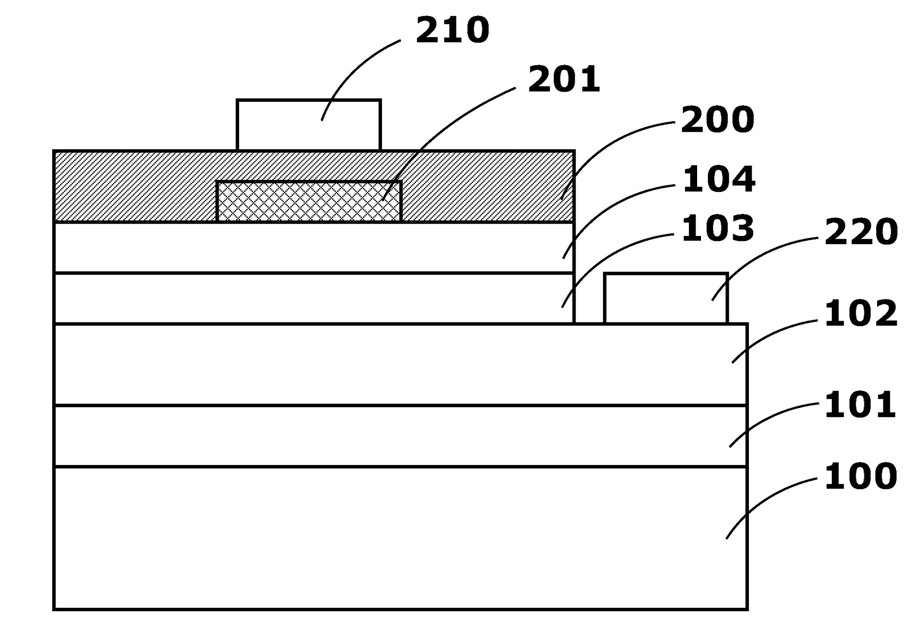
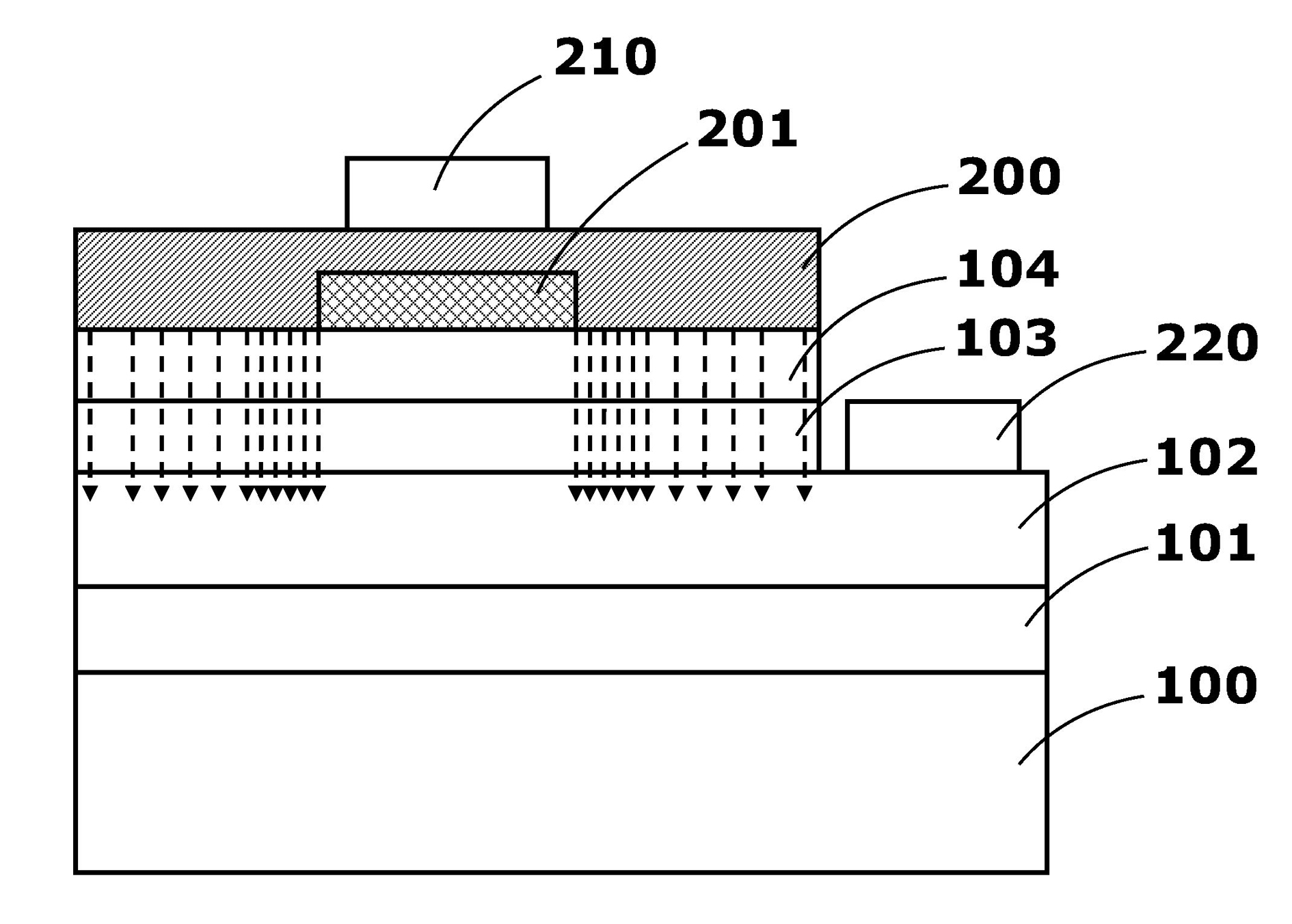
The invention discloses a light emitting diode with sandwich-type current blocking structure, comprising a sapphire substrate and a light emitting epitaxial layer, wherein the light emitting epitaxial layer is extended outwards on the sapphire substrate and is composed of an n-GaN layer, an active layer and a p-GaN layer; a first transparent conducting oxide layer is formed above the p-GaN layer;a transparent insulating layer is positioned on the first transparent conducting oxide layer and inwards retracts by 1-50 micrometers in relation to the first transparent conducting oxide layer; a second transparent conducting oxide layer covers the transparent insulating layer, outwards expands in relation to the transparent insulating layer and is electrically connected with the first transparent conducting oxide layer; a p electrode is connected with the second transparent conducting oxide layer; and an n electrode is connected with the n-GaN layer. The ''inward retraction'' positioning ofthe transparent insulating layer ensures that the current transmission mode of the first transparent conducting oxide layer is transverse transmission with certain resistance from inside to outside; thus more injected current is distributed in the outer ring area of a chip, the lighting intensity of the area is far more than that of the central area of the chip; and light extraction efficiency isimproved because the extraction probability of the photon side surface of the outer ring area of the chip is higher.

Description

technical field [0001] The invention relates to a gallium nitride-based light-emitting diode, in particular to a light-emitting diode with a sandwich-type current blocking structure. Background technique [0002] At present, gallium nitride (GaN)-based light-emitting diodes (LEDs) have been widely used in the fields of mobile phone keys, indications, displays, backlights, and lighting. The traditional gallium nitride-based light-emitting diode chip adopts a double-electrode horizontally distributed positive structure. The basic structure is to make a transparent electrode on the light-emitting epitaxial layer as an ohmic contact layer and a current spreading layer; then, on the transparent electrode. Metal electrodes (p-electrodes) are arranged for wire bonding. However, the existence of the metal electrode will cause the light emitted in the active layer to be blocked and absorbed, thereby reducing the light extraction efficiency of the LED chip. [0003] In order to avoi...

Claims


Application Information

Patent Timeline
IPC IPC(8): H01L33/14
CPCH01L33/42H01L33/145H01L21/42H01L33/40
Inventor 潘群峰吴志强林科闯黄少华
Owner XIAMEN SANAN OPTOELECTRONICS TECH CO LTD
Learn More