
Memory-cell array, nonvolatile storage device, memory-cell, and manufacturing method of memory-cell array

A memory cell array and memory cell technology, which is applied to electrical components, electric solid-state devices, circuits, etc., can solve the problems of large peripheral circuit ratio, large leakage current, and obstacles to the high integration of non-volatile memory devices, and achieve electric Excellent characteristics, prevention of leakage paths, and high integration

Active Publication Date: 2013-01-23
PANASONIC SEMICON SOLUTIONS CO LTD
View PDF1 Cites 0 Cited by
  • Summary
  • Abstract
  • Description
  • Claims
  • Application Information

AI Technical Summary

Problems solved by technology

[0020] Accordingly, when the matrix size of the memory cell array cannot be increased due to the large leakage current of the diode, the ratio of the area of ​​the peripheral circuit to the area of ​​the memory cell array has to be relatively large.
As a result, high integration of nonvolatile memory devices is hindered

Method used


Image

  • Memory-cell array, nonvolatile storage device, memory-cell, and manufacturing method of memory-cell array
  • Memory-cell array, nonvolatile storage device, memory-cell, and manufacturing method of memory-cell array
  • Memory-cell array, nonvolatile storage device, memory-cell, and manufacturing method of memory-cell array

Examples


Embodiment approach 1

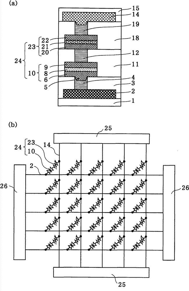
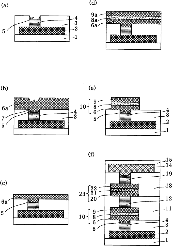
[0091] use Figure 1 to Figure 2 A memory cell array using a nonvolatile memory element in which a variable resistance element and a diode are connected in series and a method for manufacturing the memory cell array according to Embodiment 1 of the present invention are described. formed by connection.

[0092] figure 1 (a) is a schematic cross-sectional view showing an example of the structure of one memory cell used in the memory cell array according to Embodiment 1 of the present invention. figure 1 (b) is a block diagram showing an example of a functional configuration of a nonvolatile memory device configured by arranging these memory cells in a matrix.

[0093] Such as figure 1 As shown in (a), the memory cell of the first embodiment is formed on the semiconductor substrate 1 . For example, semiconductor substrate 1 is composed of a silicon substrate. A first conductor layer 2 is formed above a semiconductor substrate 1 , and a first interlayer insulating film 3 is ...

Embodiment approach 2

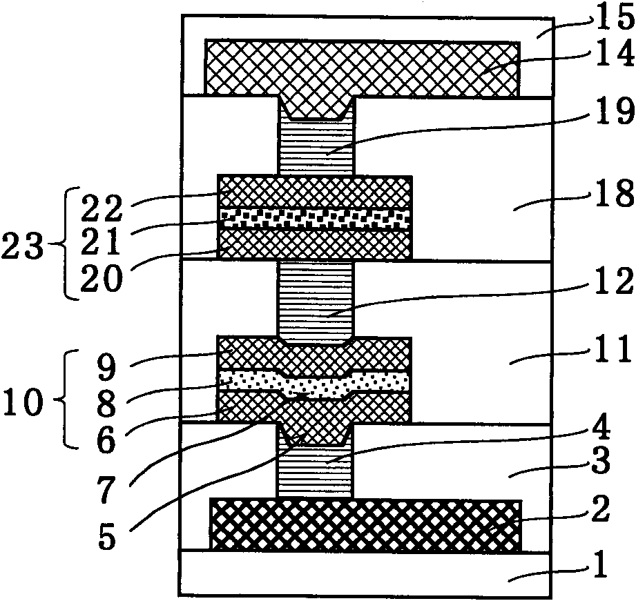
[0133] For the memory cell according to Embodiment 2 of the present invention, using Figure 3 to Figure 4 Be explained.

[0134] image 3 It is a schematic cross-sectional view showing an example of the structure of the memory cell according to the second embodiment.

[0135] Such as image 3 As shown, the memory cell of the second embodiment is different from the memory cell of the first embodiment in that the upper surface of the first electrode 6 located directly above the first plug 4 is concave toward the substrate. This recess is called a second recess 7 . The depth of the second concave portion 7 is formed smaller than the depth of the first concave portion 5 .

[0136] Compared with the memory cell of Embodiment 1, the memory cell of Embodiment 2 has the second recess 7 on the top of the first electrode 6, and the current control layer 8 and the second electrode 9 located on the top of the second recess 7 Except for the difference in shape, the number of laminate...

Embodiment approach 3

[0152] For the memory cell according to Embodiment 3 of the present invention, using Figure 5 to Figure 6 Be explained.

[0153] Figure 5 It is a schematic cross-sectional view showing an example of the structure of the memory cell according to the third embodiment.

[0154] Such as Figure 5 As shown, the memory cell of the third embodiment shares the second electrode 9 of the current steering element 10 and the lower electrode 20 of the variable resistance element 23 in the memory cell of the first embodiment, so that the current steering element 10 and the variable resistance element 23 formed as one. Furthermore, the second interlayer insulating film 11 and the second plug 12 in the memory cell of Embodiment 1 are omitted.

[0155] The structure of the memory cell of Embodiment 3 is the same as the structure of the memory cell of Embodiment 1 except for the differences described above. Hereinafter, for convenience of explanation, the respective constituent elements ...


PUM


Abstract

A method of manufacturing a memory cell array in which first conductive layers (2) and second conductive layers (14) extend above a semiconductor substrate (1) and three-dimensionally cross with each other, and memory cells each of which includes a current steering element (10) and a variable resistance element (23) electrically connected in series to each other is provided at a corresponding one of three-dimensional cross points between the first conductive layers (2) and the second conductive layers (14). The method includes: forming a first interlayer insulating film (3); forming a contact hole in the interlayer insulating film (3); depositing a first plug material (4) in the contact hole and on the first interlayer insulating film (3); performing a first polishing in which the first plug material (4) is polished until the first interlayer insulating film (3) is exposed; depositing a conductive film (6a) that becomes a first electrode (6) of the current steering element (10), on the first plug material (4) and the first interlayer insulating film (3) after the first polishing; and performing a second polishing in which a surface of the conductive film (6a) is polished.

Description

technical field [0001] The present invention relates to a memory cell array using a nonvolatile memory element that controls a variable resistance element and a current flowing through the variable resistance element, and a method for manufacturing the same, as a memory cell. The current control elements are connected in series. Background technique [0002] In recent years, research on variable resistance elements that store information by using the memory function of the variable resistance layer has been active. [0003] The variable resistance layer used in this variable resistance element is a thin film composed of a material mainly composed of metal oxide. When a voltage pulse is applied to the resistance variable layer, its resistance value changes, and the changed resistance value is held in a non-volatile manner. If the high-resistance state and the low-resistance state of the resistance variable layer are respectively associated with, for example, "1" and "0" of ...

Claims


Application Information

Patent Timeline
Patent Type & Authority Patents(China)
IPC IPC(8): H01L27/10H01L45/00H01L49/00H10N99/00
CPCH01L45/08H01L27/2418H01L27/24H01L45/146H01L27/101H01L45/145H01L45/1625H01L45/1233H10B63/22H10N70/24H10N70/826H10N70/8833H10N70/026
Inventor 冈田崇志三河巧有田浩二
Owner PANASONIC SEMICON SOLUTIONS CO LTD
Learn More