Method for modeling P-channel metal oxide semiconductor (PMOS) one-time programmable memory (OTP) device
A modeling method and device technology, which can be used in instruments, special data processing applications, electrical digital data processing, etc., and can solve problems such as small area and short writing time.
- Summary
- Abstract
- Description
- Claims
- Application Information
AI Technical Summary
Problems solved by technology
Method used
Image

Examples
Embodiment Construction
[0016] like image 3 Shown is the flowchart of the modeling method of PMOS OTP device of the present invention, and the present invention comprises the steps:
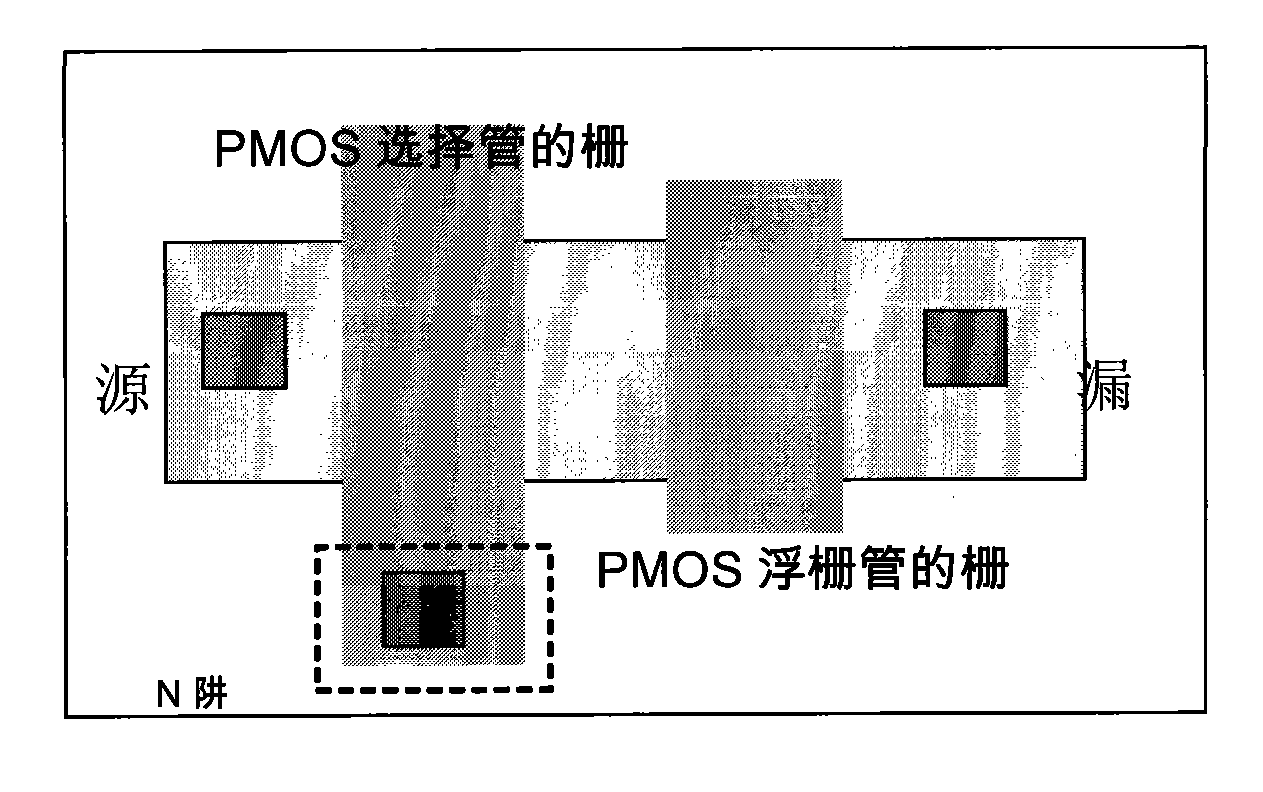
[0017] Step 1. Establish a set of equivalent circuits according to the structure and working principle of the PMOS OTP device. like Figure 4 As shown, the equivalent circuit structure includes: a PMOS selection transistor, a PMOS floating gate transistor, the PMOS selection transistor and the PMOS floating gate transistor form a series structure in which the drain end of the PMOS selection transistor is connected to the source end of the PMOS floating gate transistor The body potential of the PMOS selection transistor and the PMOS floating gate transistor is connected in series, the source terminal of the PMOS selection transistor is connected to the source voltage, and the gate is connected to the gate voltage; the drain terminal of the PMOS floating gate transistor is connected to the drain voltage, and the drain t...
PUM
 Abstract
Description
Claims
Application Information
 - R&D
- Intellectual Property
- Life Sciences
- Materials
- Tech Scout
- Unparalleled Data Quality
- Higher Quality Content
- 60% Fewer Hallucinations
Browse by: Latest US Patents, China's latest patents, Technical Efficacy Thesaurus, Application Domain, Technology Topic, Popular Technical Reports.
© 2025 PatSnap. All rights reserved.Legal|Privacy policy|Modern Slavery Act Transparency Statement|Sitemap|About US| Contact US: help@patsnap.com