
Conductive structure and integrated circuit assembly

A technology of conductive structures and devices, applied in the direction of electric solid devices, semiconductor devices, circuits, etc., can solve the problems of increased deposition thickness, increased manufacturing cost, increased metal layer thickness, etc., and achieves reduced thickness and reduced manufacturing cost. , the effect of high yield

Active Publication Date: 2011-06-01
SAMSUNG ELECTRONICS CO LTD
View PDF6 Cites 0 Cited by
  • Summary
  • Abstract
  • Description
  • Claims
  • Application Information

AI Technical Summary

Problems solved by technology

In order to completely fill the opening, the deposited thickness of the metal layer and thus the thickness of the metal layer to be removed can also be increased, thereby increasing the manufacturing cost
Often, openings may not be sufficiently and completely filled with metal layers, which can lead to defects

Method used


Image

  • Conductive structure and integrated circuit assembly
  • Conductive structure and integrated circuit assembly
  • Conductive structure and integrated circuit assembly

Examples


Embodiment approach 1

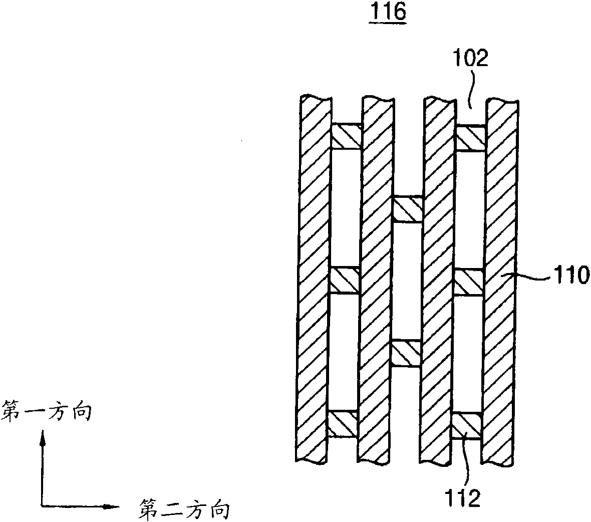
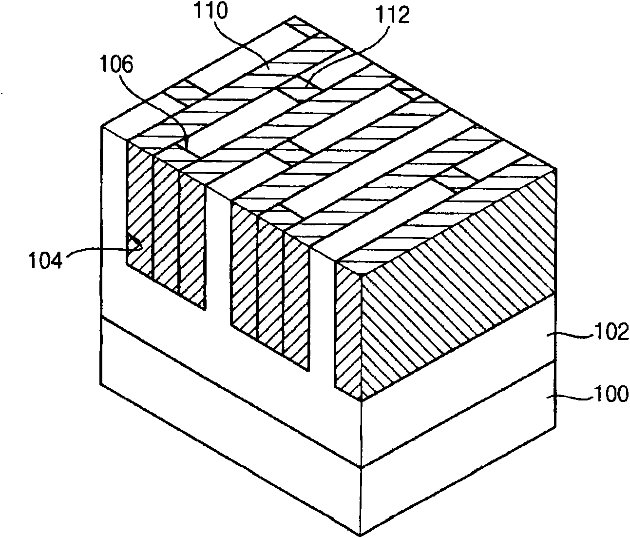
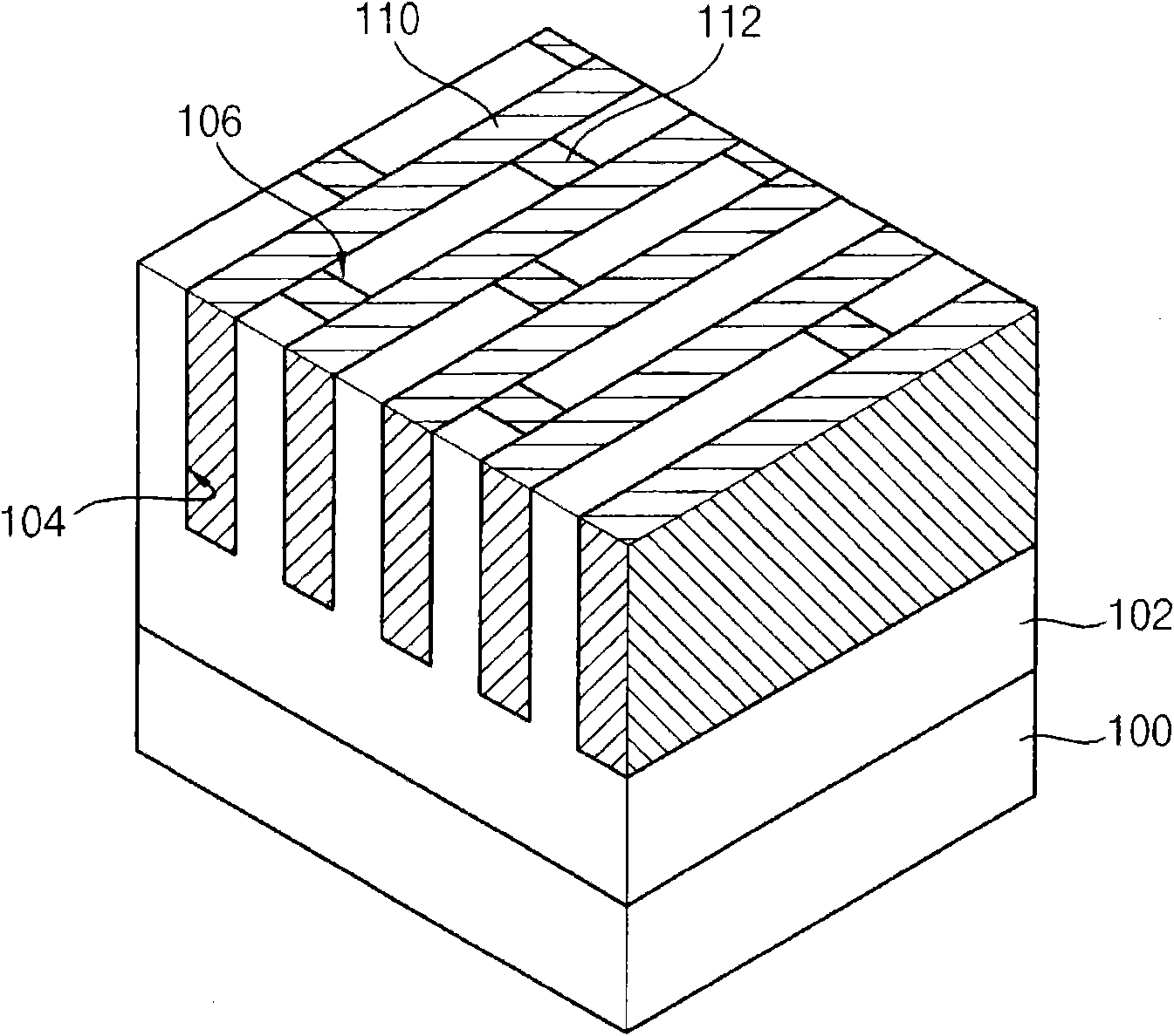
[0062] figure 1 is a plan view illustrating a conductive pattern structure according to an exemplary embodiment. figure 2 is a perspective view showing figure 1 The conductive pattern structure shown. image 3 is another perspective view showing figure 1 The conductive pattern structure shown.

[0063] cable in figure 2 is shown in cross-section in the perspective view, however, the connecting lines are not in the image 3 The cross-section in the perspective view is shown.

[0064] refer to Figure 1 to Figure 3 The conductive pattern structure 116 may include a mold layer 102 formed on the substrate 100 using an insulating material. A plurality of first grooves 104 may be formed at the mold layer 102 parallel to each other. A plurality of second trenches 106 may be formed penetrating portions of sidewalls of the mold layer 102 protruding between the plurality of first trenches 104 . Each second trench 106 may penetrate into some portion of the sidewall of the m...

Embodiment approach 2

[0105] Figure 9 is a plan view showing a conductive pattern structure according to Exemplary Embodiment 2. FIG.

[0106] refer to Figure 9 , a mold layer 150 of insulating material may be formed on the substrate.

[0107] A plurality of first grooves 152 having a first width W1 may be formed at the mold layer 150 substantially parallel to each other along a first direction. Second trenches 154 may be formed penetrating portions of sidewalls of the mold layer 150 between the first trenches 152 . Each second groove 154 may penetrate the protruding mold layer 150 between two adjacent first grooves 152 . The second width W2 of the second trench 154 along the first direction may be the same as or smaller than the first width W1. The first groove 152 and the second groove 154 may have the same depth.

[0108] One or more third grooves 156 having a third width and disposed parallel to each other may be formed in the mold layer 150 .

[0109]The first width W1, the second widt...

Embodiment approach 3

[0127] Figure 13 is a plan view showing a conductive pattern structure according to Exemplary Embodiment 3. FIG. Figure 14 is a perspective view showing Figure 13 The conductive pattern structure shown.

[0128] refer to Figure 13 and Figure 14 , a mold layer 202 of insulating material may be formed on the substrate 200 . The mold layer 202 may have a stacked structure of a first silicon oxide layer 202a, an etch stop layer 202b, and a second silicon oxide layer 202c. In the mold layer 202, a contact hole 204 and trenches 206, 208, and 210 may be formed.

[0129] In particular, a contact hole 204 exposing a portion of the surface of the substrate 200 may be formed through the mold layer 202 . The contact holes 204 may be disposed along the first direction.

[0130] A first trench 206 connected to the contact hole 204 and extending in a first direction may be formed in a portion of the mold layer 202 including the contact hole 204 . The first trench 206 may have a ...


PUM


Abstract

The invention provides a conductive structure and an integrated circuit assembly. The conductive structure includes a contact plug extending through an insulating layer on a substrate, and first and second conductive lines extending alongside one another on the insulating layer. The first conductive line extends on the contact plug. A connecting line on the insulating layer extends between and electrically connects the first and second conductive lines. Related integrated circuit devices and fabrication methods are also discussed.

Description

technical field [0001] Exemplary embodiments relate to conductive pattern structures and methods of manufacturing the same. More particularly, exemplary embodiments relate to a conductive pattern structure including a metal material and a method of manufacturing the same. Background technique [0002] As semiconductor devices become more highly integrated, wiring of semiconductor devices may need to have smaller or narrower pattern widths and / or lower resistance. Therefore, metal materials having low resistance have been used to form wirings. Such metal wiring may be difficult to form by patterning with a photolithography process. Therefore, a damascene process has been used to form metal wirings. [0003] When a metal wiring having a wider pattern width is formed by a damascene process, metal may be deposited to completely fill an opening formed for forming the wiring. The metal layer formed on the area outside the opening is removed. In order to completely fill the op...

Claims


Application Information

Patent Timeline
Patent Type & Authority Applications(China)
IPC IPC(8): H01L23/522H01L23/528
CPCH01L23/528H01L21/76816H01L21/76807H01L27/11521H01L27/11524H01L2924/0002H10B41/30H10B41/35H01L2924/00H01L21/28
Inventor 权炳昊尹普彦
Owner SAMSUNG ELECTRONICS CO LTD
Learn More