ESD (electrostatic discharge) protection circuit and manufacturing method thereof

A technology of ESD protection and manufacturing method, which can be used in circuits, semiconductor/solid-state device manufacturing, electrical components, etc., and can solve the problem of high process cost

Inactive Publication Date: 2011-06-01
SHANGHAI HUA HONG NEC ELECTRONICS
View PDF0 Cites 12 Cited by
  • Summary
  • Abstract
  • Description
  • Claims
  • Application Information

AI Technical Summary

Problems solved by technology

Usually, the ESD protection circuit formed by TVS (Transient Voltage Suppressor, transient voltage suppression) diodes contains capacitors made of s

Method used


Image

  • ESD (electrostatic discharge) protection circuit and manufacturing method thereof
  • ESD (electrostatic discharge) protection circuit and manufacturing method thereof
  • ESD (electrostatic discharge) protection circuit and manufacturing method thereof

Examples


Example Embodiment

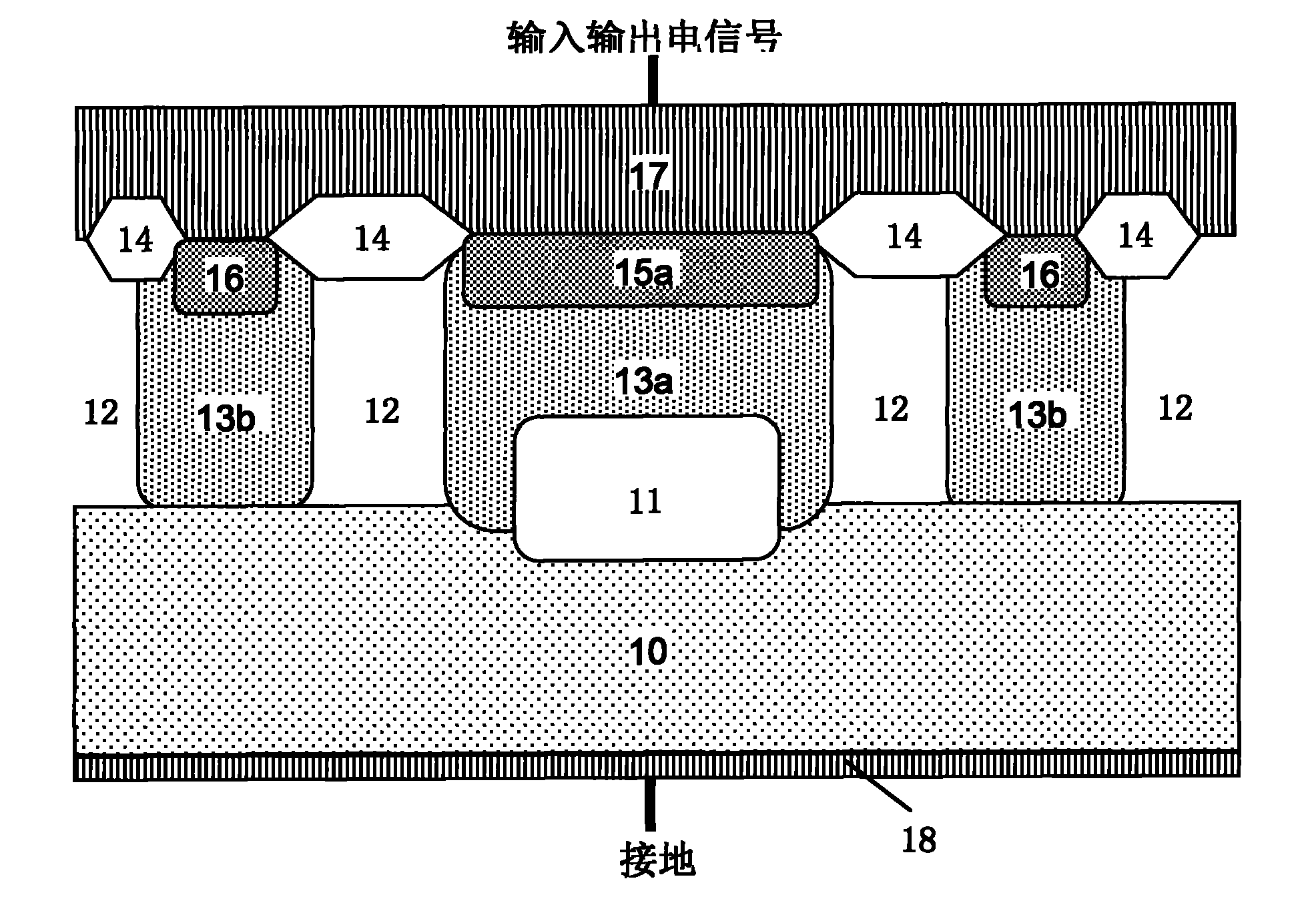
[0021] see figure 1 , the structure of the ESD protection circuit of the present invention is: a p-type epitaxial layer 12 is formed on the p-type heavily doped substrate 10 . There are at least two independent n-wells 13a, 13b in the p-type epitaxial layer 12 and / or the p-type heavily doped substrate 10 . "Independent" means that there is no overlap between two or more wells. The top of the n-wells 13a and 13b is the upper surface of the p-type epitaxial layer 12, and the bottom is the lower surface of the p-type epitaxial layer 12 or the p-type heavily doped substrate 10 below. The upper surface of the p-type epitaxial layer 12 has a plurality of isolation regions 14, and the isolation regions 14 at least isolate the n-wells 13a and 13b from each other. There is an n-type heavily doped Zener ion implantation region 11 in the n-well 13a and / or the p-type heavily doped substrate 10. The top of the n-type heavily doped Zener ion implantation region 11 is in the n-well 13a, an...


PUM

PropertyMeasurementUnit
Thicknessaaaaaaaaaa

Abstract

The invention discloses an ESD (electrostatic discharge) protection circuit. The protection circuit is composed of a first branch and a second branch which are connected in parallel, wherein the first branch is formed by connecting a Zener diode (21) with a first diode (22) in serials; and the second branch is a second diode (23). The protection circuit is characterized in that an n-type heavily doped Zener ion implantation region (11) and a p-type heavily doped substrate (10) form the Zener diode (21); a p-type heavily doped region (15a) and an n well (13a) form the first diode (22); and an n well (13b) and the p-type heavily doped substrate (10) form the second diode (23). The invention also discloses a manufacturing method of the ESD protection circuit. The ESD protection circuit has the advantages of low parasitic capacitance and high response speed, is simple to manufacture, and is especially suitable for protection of input/output ESD circuits with voltages lower than 5V.

Description

technical field [0001] The invention relates to a circuit ESD (Electrostatic Discharge, electrostatic discharge) protection circuit. Background technique [0002] The ESD protection circuit formed by using diodes pays more attention to the parasitic capacitance introduced by diodes, especially when applied to high-speed circuits. The smaller the parasitic capacitance introduced by the diode, the faster the response. Generally, the ESD protection circuit formed by TVS (Transient Voltage Suppressor, transient voltage suppressor) diodes contains capacitors made of shallow trenches. The disadvantage of this structure is that it requires additional process steps that can be shallow trenches, and the process cost is high. SUMMARY OF THE INVENTION [0003] The technical problem to be solved by the present invention is to provide an ESD protection circuit that only introduces a small parasitic capacitance and does not require a process step of etching trenches. [0004] In order...

Claims


Application Information

Patent Timeline
IPC IPC(8): H01L27/08H01L29/06H01L21/77H01L21/265H01L23/60
Inventor 张帅戚丽娜
Owner SHANGHAI HUA HONG NEC ELECTRONICS
Why Eureka
Try Eureka