

Method for enhancing welding reliability of high-frequency quad flat no lead (QFN) device
A reliability and device technology, which is applied in the field of reliable welding of high-frequency QFN devices, can solve problems such as QFN device failure, increased solder joint stress, and increased assembly stress, so as to solve the problem of increased welding stress, reduced thermal stress, and reduced The effect of welding stress
- Summary
- Abstract
- Description
- Claims
- Application Information
AI Technical Summary
Problems solved by technology
Method used
Image

Examples
Embodiment 1
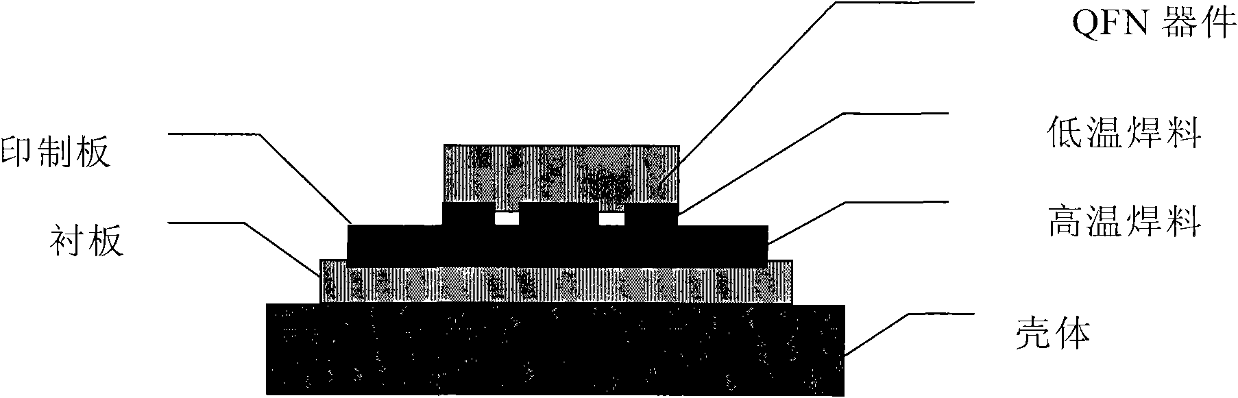
[0032] The assembly method designed by the present invention is adopted, that is, a liner is added between the printed board and the shell, and the material of the liner is brass H62 (thermal expansion coefficient 16ppm / °C), with a thickness of 2mm. The number of test pieces is 4 pieces, numbered B01~B04.
[0033] 1. Basic conditions
[0034] (1) Printed board
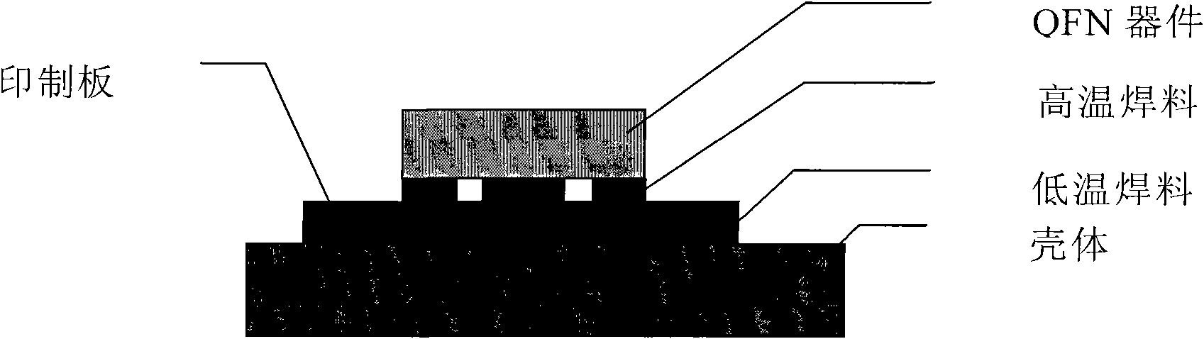
[0035] In order to effectively verify the soldering quality of QFN devices, the printed board in this embodiment strives to be simplified to avoid introducing other factors, such as Figure 4 Shown is a schematic structural diagram of the printed board of the present invention. In the figure, it can be clearly seen that the surrounding pin pads and the belly ground pads of the printed board correspond to the QFN device. The printed board is made of Rogers4350B and has a thickness of 0.254mm.
[0036] (2) Components
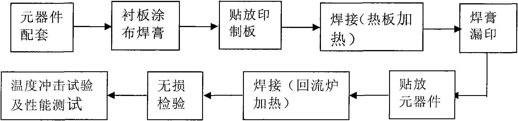
[0037] According to the printed board design, the supporting components of a single test piece are s...
Embodiment 2
[0076] The assembly method designed by the present invention is adopted, that is, a liner is added between the printed board and the shell, and the material of the liner is Kefa alloy (thermal expansion coefficient 8ppm / °C). The number of test pieces is 4 pieces, numbered C01~C04.
[0077] 1. Basic conditions
[0078] (1) Printed board
[0079] Same as "Example" 1.
[0080] (2) Components
[0081] Same as "Example 1".
[0082] (3) Solder and flux
[0083] Same as "Example 1".
[0084] (4) Production and testing tools and equipment
[0085] Same as "Example 1".
[0086] Two, process implementation steps
[0087] Step (1), supporting components
[0088] Same as "Example 1".
[0089] Step (2),
[0090] Same as "Example 1".
[0091] Step (3),
[0092] Same as "Example 1".
[0093] Step (4),
[0094] Same as "Example 1".
[0095] Step (5), solder paste leakage
[0096] Same as "Example 1".
[0097] Step (6) patch
[0098] Same as "Example 1".
[0099] Step (7), ...
Embodiment 3
[0108] The assembly method designed by the present invention is adopted, that is, a liner is added between the printed board and the shell, and the material of the liner is Kefa alloy (thermal expansion coefficient 8ppm / °C). Control the amount of solder paste coating on the solder joints of the device by adjusting the opening size of the slab. Choose a 0.15mm thick slab. The opening size of the slab shrinks appropriately relative to the size of the pad. The shrinkage ratio is: 70% of the surrounding pin pads 4 test pieces with 65% grounding pads on the abdomen, numbered D01-D04; 4 test pieces with 56% lead pads around the abdomen and 51% grounding pads on the abdomen, numbered D05-D08.
[0109] 1. Basic conditions
[0110] (1) Printed board
[0111] Same as "Example 1".
[0112] (2) Components
[0113] Same as "Example 1".
[0114] (3) Solder and flux
[0115] Same as "Example 1".
[0116] (4) Production and testing tools and equipment
[0117] No. 2 leak board: thickne...
PUM
| Property | Measurement | Unit |
|---|---|---|
| Melting point | aaaaa | aaaaa |
| Melting point | aaaaa | aaaaa |
| Thickness | aaaaa | aaaaa |
Abstract
Description
Claims
Application Information