

Nitride light emitting diode having composite double current spreading layer
A technology of light-emitting diodes and current expansion layers, which is applied in circuits, electrical components, semiconductor devices, etc., can solve the problems of high current density, current crowding, and effective improvement of the limited light efficiency level, so as to improve the electrostatic breakdown voltage and avoid Effect of current crowding and improvement of luminous efficiency
Active Publication Date: 2011-06-15
XIAMEN SANAN OPTOELECTRONICS TECH CO LTD
View PDF4 Cites 23 Cited by
- Summary
- Abstract
- Description
- Claims
- Application Information
AI Technical Summary
Problems solved by technology
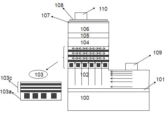
Because the electrodes flowing from the n-electrode 109 to the p-electrode 108 will be biased towards the closer line, this will cause excessive current density in some parts, resulting in current crowding, thus limiting the effective improvement of the light efficiency level
Method used
View moreImage
Smart ImageViewing Examples

Examples
Embodiment 1
Embodiment 2
Login to View More PUM
 Abstract
The invention discloses a nitride light emitting diode having a composite double current spreading layer. The composite double current spreading layer is a composite semiconductor layer which consists of a first current spreading layer and a second current spreading layer in a sequentially superposed manner; the first current spreading layer is formed on a distribution insulated layer of an n-type nitride semiconductor layer and the second current spreading layer is formed by mutually superposing u-type nitride semiconductor layers and n-type nitride semiconductor layers; and the composite double current spreading layer is connected with the n-type nitride semiconductor layers and an active layer respectively. In the composite double current spreading layer arranged on the nitride light emitting diode, the current can be distributed over the entire light emitting area quite evenly to avoid current crowding, therefore, both the light emitting efficiency of a nitride light emitting diode assembly and the electrostatic breakdown voltage can be raised effectively.
Description
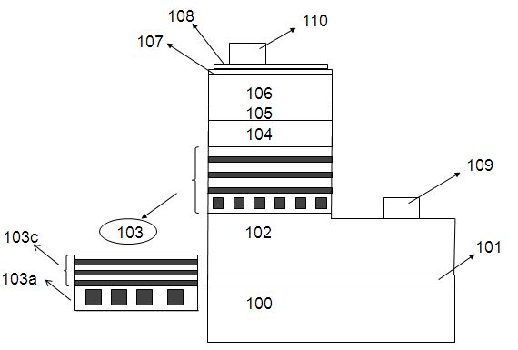
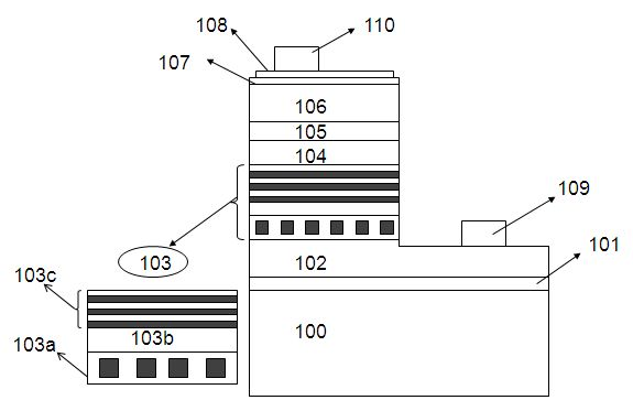
Nitride light-emitting diode with composite double current spreading layer Technical field The invention relates to a nitride semiconductor light-emitting device, more specifically a nitride light-emitting diode with a compound current spreading layer (Compound current spreading layer). Background technique In recent years, the development of semiconductor lighting technology represented by nitride semiconductor materials has attracted widespread attention worldwide. With the continuous improvement of epitaxy and chip technology, the luminous efficiency of nitride light-emitting diodes has been continuously improved. However, to truly popularize semiconductor lighting, it still needs to continue to improve on the existing level of light efficiency. Figure 1 is a schematic diagram of the structure of a general nitride light-emitting diode and a schematic diagram of its current path. A buffer layer 101, an n-type nitride semiconductor layer 102, a light-emitting layer 104, a p-...
Claims
Login to View More Application Information
Patent Timeline
 Patent Type & AuthorityApplications(China)
IPC IPC(8): H01L33/14H01L33/12H01L33/00
CPCH01L33/14H01L33/025H01L33/32H01L33/007H01L33/145
Inventor叶孟欣吴志强黄少华周启伦吕兴维林科闯
OwnerXIAMEN SANAN OPTOELECTRONICS TECH CO LTD