
Organic light-emitting device and production method thereof

An electroluminescent device and a luminescent technology, which are applied in the fields of electric solid-state devices, semiconductor/solid-state device manufacturing, electrical components, etc., can solve the high requirements for doping concentration and doping thickness control, and the preparation of doped intermediate connection layers. Problems such as complex process and unfavorable mass production achieve the effects of reducing current density, simplifying the preparation process and controlling costs, and improving luminous efficiency and lifespan

Inactive Publication Date: 2011-06-15
UNIV OF ELECTRONIC SCI & TECH OF CHINA
View PDF4 Cites 12 Cited by
  • Summary
  • Abstract
  • Description
  • Claims
  • Application Information

AI Technical Summary

Problems solved by technology

This type of structure can effectively improve the efficiency and life of the device. However, the preparation process of the doped intermediate connection layer is relatively complicated, and the control of doping concentration and doping thickness is very demanding, which not only increases the cost, but also is not conducive to mass production. Production

Method used


Image

  • Organic light-emitting device and production method thereof
  • Organic light-emitting device and production method thereof
  • Organic light-emitting device and production method thereof

Examples


Embodiment 1

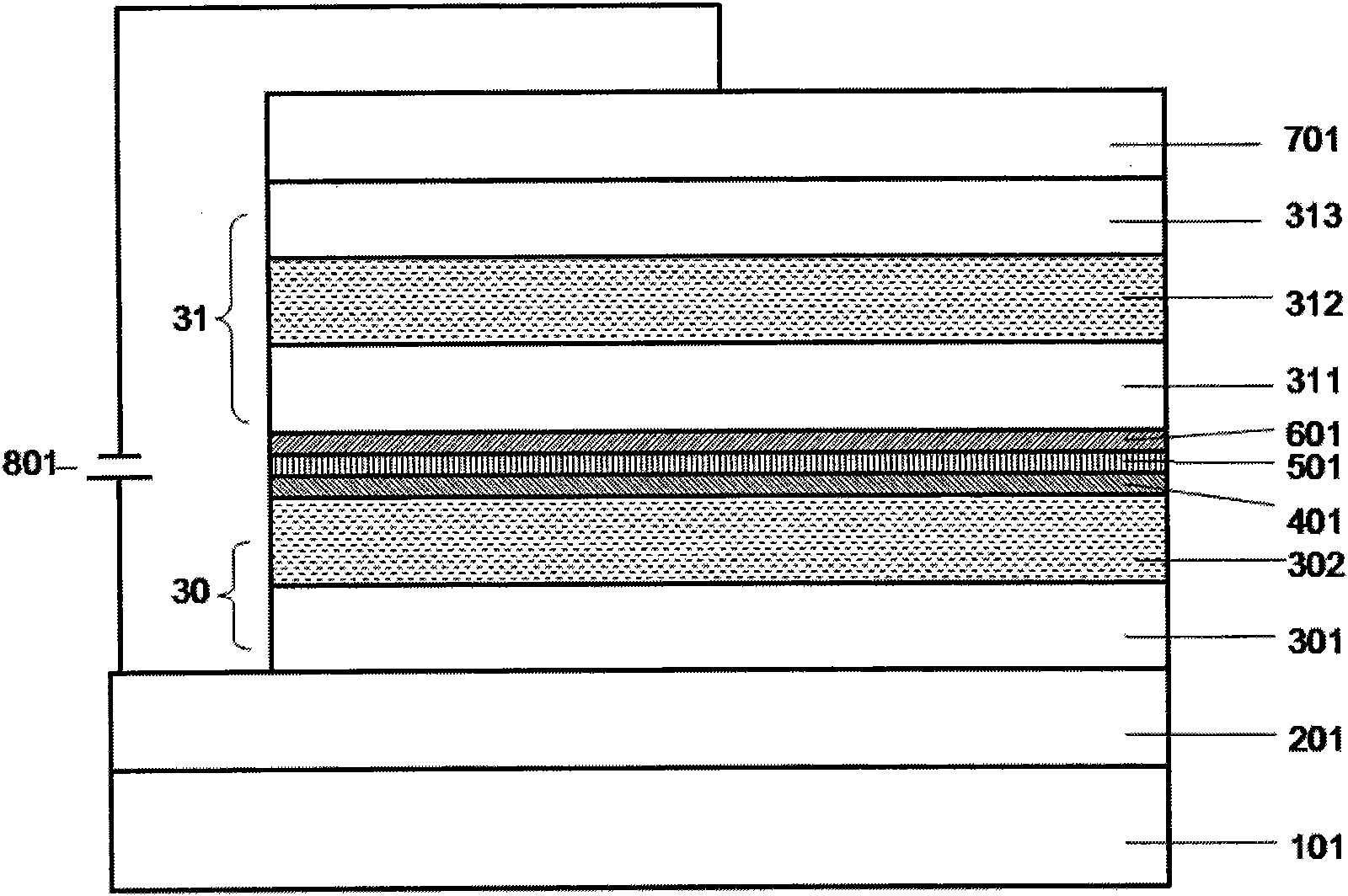
[0099] Such as figure 2 As shown, the ultra-thin connection layer in the structure of the device includes an organic ultra-thin layer 401 as a buffer layer, an N-type metal ultra-thin layer 501 , and a P-type metal compound ultra-thin layer 601 .

[0100] The organic ultra-thin layer of the device as a buffer layer is Bphen, the N-type metal ultra-thin layer is Mg, and the P-type metal compound ultra-thin layer is V 2 o 5 .

[0101] The first electroluminescent unit 30 in the structure of the device includes a hole transport layer 301 and a doped layer 302 that emits blue light.

[0102] The second electroluminescent unit 31 in the structure of the device includes a hole transport layer 311 , a doped layer 312 emitting blue light, and an electron transport layer 313 .

[0103] The blue-emitting phosphorescent material of the device is FIrPic, the phosphorescent host material is CBP, the hole transport material is NPB, and the electron transport material is Alq 3 , The cat...

Embodiment 2

[0118] Such as figure 2 As shown, the ultra-thin connection layer in the structure of the device includes an organic ultra-thin layer 401 as a buffer layer, an N-type metal ultra-thin layer 501 , and a P-type metal compound ultra-thin layer 601 .

[0119] The organic ultra-thin layer of the device as a buffer layer is CuPc, the N-type metal ultra-thin layer is Li, and the P-type metal compound ultra-thin layer is FeCl 3 .

[0120] The first electroluminescent unit 30 in the structure of the device includes a hole transport layer 301 and a doped layer 302 that emits green light.

[0121] The second electroluminescent unit 31 in the structure of the device includes a hole transport layer 311 , a doped layer 312 emitting green light, and an electron transport layer 313 .

[0122] The phosphorescent material of the device that emits green light is Ir(ppy) 3 , the phosphorescent main material is UGH2, the hole transport material NPB, the electron transport material TPBi, and th...

Embodiment 3

[0126] Such as figure 2 As shown, the ultra-thin connection layer in the structure of the device includes an organic ultra-thin layer 401 as a buffer layer, an N-type metal ultra-thin layer 501 , and a P-type metal compound ultra-thin layer 601 .

[0127] The organic ultra-thin layer of the device as a buffer layer is BCP, the N-type metal ultra-thin layer is Ca, and the P-type metal compound ultra-thin layer is M O o 3 .

[0128] The first electroluminescent unit 30 in the structure of the device includes a hole transport layer 301 and a doped layer 302 that emits red light.

[0129] The second electroluminescent unit 31 in the structure of the device includes a hole transport layer 311 , a doped layer 312 emitting red light, and an electron transport layer 313 .

[0130] The red-emitting phosphorescent material of the device is Ir(piq) 3 , the phosphorescent main material is MCP, the hole transport material NPB, the electron transport material TPBi, and the cathode laye...


PUM

PropertyMeasurementUnit
Thicknessaaaaaaaaaa
Thicknessaaaaaaaaaa
Sheet resistanceaaaaaaaaaa

Abstract

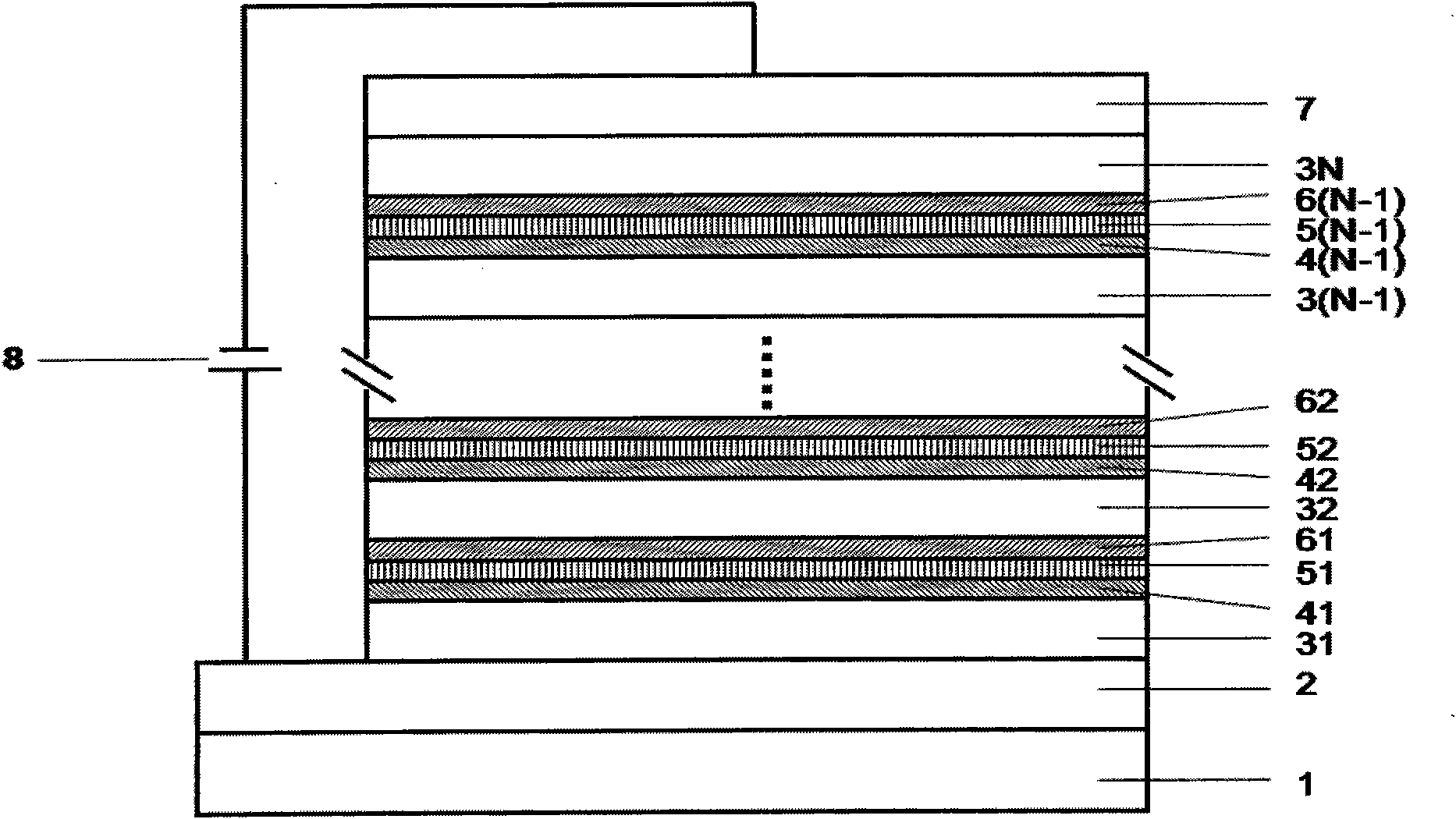
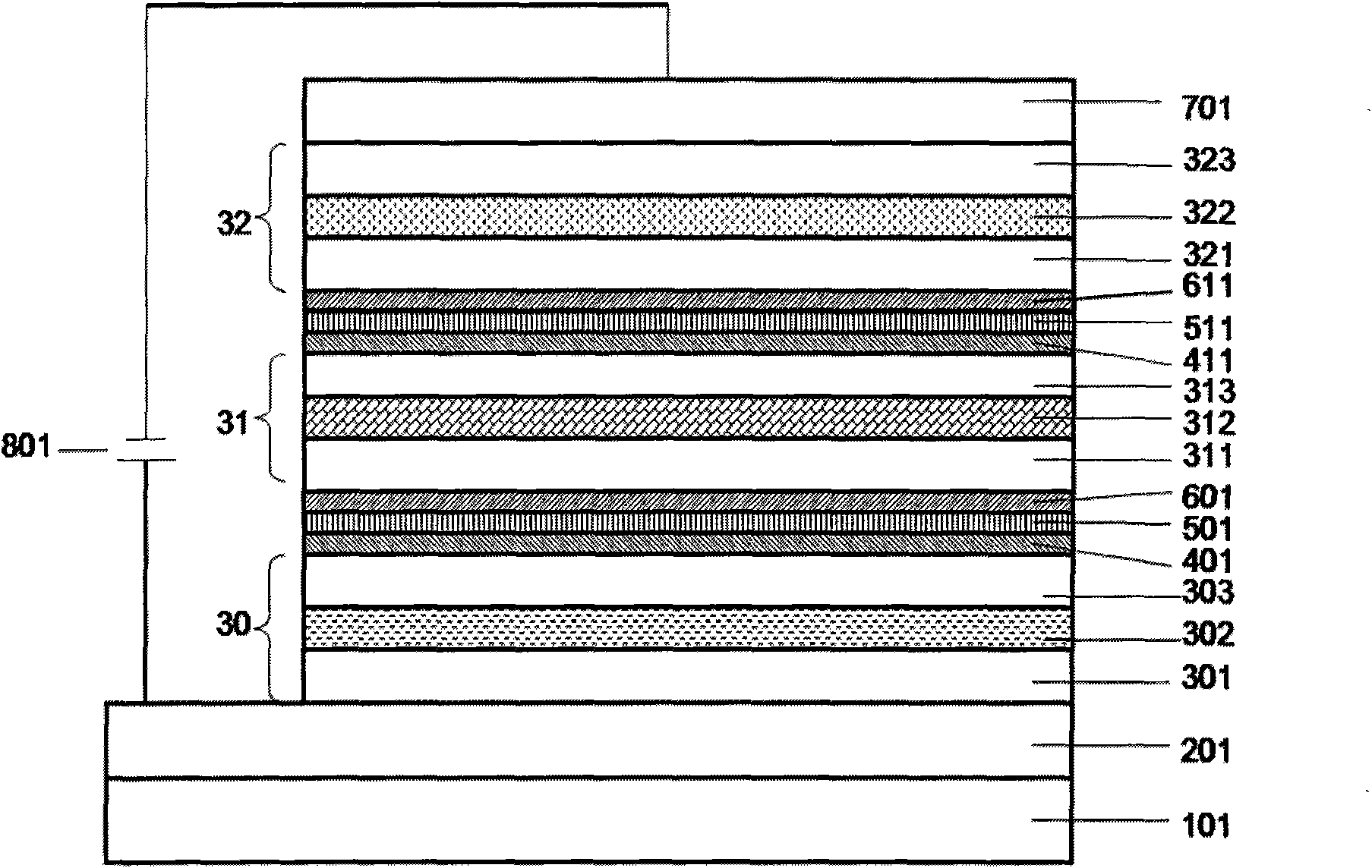
The invention discloses an organic light-emitting device, which comprises a substrate, an anode layer, a cathode layer, at least two light-emitting units and at least one intermediate junction layer, wherein the at least two light-emitting units and the at least one intermediate junction layer are arranged between the anode layer and the cathode layer; and an electrode is positioned on the surface of the transparent substrate. The organic light-emitting device is characterized in that: the intermediate junction layer is positioned between two adjacent light-emitting units, and comprises an organic ultrathin layer, an ultrathin metal layer and an ultrathin metal compound layer; the ultrathin metal layer is positioned between the organic ultrathin layer and the ultrathin metal compound layer; the organic ultrathin layer is a buffer layer; the ultrathin metal layer is an N-type layer; and the ultrathin metal compound layer is a P-type layer. The three undoped ultrathin layers are introduced into the structure of the intermediate junction layer so as to simplify an intermediate junction layer production process, improve the production efficiency of the device and obtain the organic light-emitting device with high luminous efficiency and long service life under low current density drive.

Description

technical field [0001] The invention relates to the technical field of organic electroluminescence in electronic components, in particular to an organic electroluminescence device with an ultra-thin connection layer structure. Background technique [0002] Organic electroluminescence refers to the phenomenon that organic light-emitting materials emit light under the excitation of electric current or electric field. In 1963, Pope et al. (J.Chem.Phys., 1963, 38, 2042) of New York University reported the electroluminescence phenomenon of organic material single crystal anthracene for the first time, which opened the prelude to the research of organic electroluminescence. In 1982, Vincett's research group (Thin SolidFilms, 1982, 94, 171) successfully prepared an anthracene single crystal film with a thickness of 0.6 μm by vacuum evaporation method, and lowered the operating voltage of organic electroluminescence to within 30V. By 1987, C.W.Tang and S.A.Vanslyke (Appl.Phys.lett....

Claims


Application Information

Patent Timeline
IPC IPC(8): H01L51/50H01L51/52H01L51/56
Inventor 于军胜文雯马柱蒋亚东
Owner UNIV OF ELECTRONIC SCI & TECH OF CHINA
Learn More