Illumination system of a microlithographic projection exposure apparatus

An illumination system, microlithography technology, applied in the system field

Active Publication Date: 2013-05-29
CARL ZEISS SMT GMBH
View PDF7 Cites 0 Cited by
  • Summary
  • Abstract
  • Description
  • Claims
  • Application Information

AI Technical Summary

Problems solved by technology

A field stop typically consists of multiple blades that can be moved individually to limit the field of illumination in the mask

Method used


Image

  • Illumination system of a microlithographic projection exposure apparatus
  • Illumination system of a microlithographic projection exposure apparatus
  • Illumination system of a microlithographic projection exposure apparatus

Examples


Embodiment Construction

[0053] I. Overall structure of projection exposure equipment

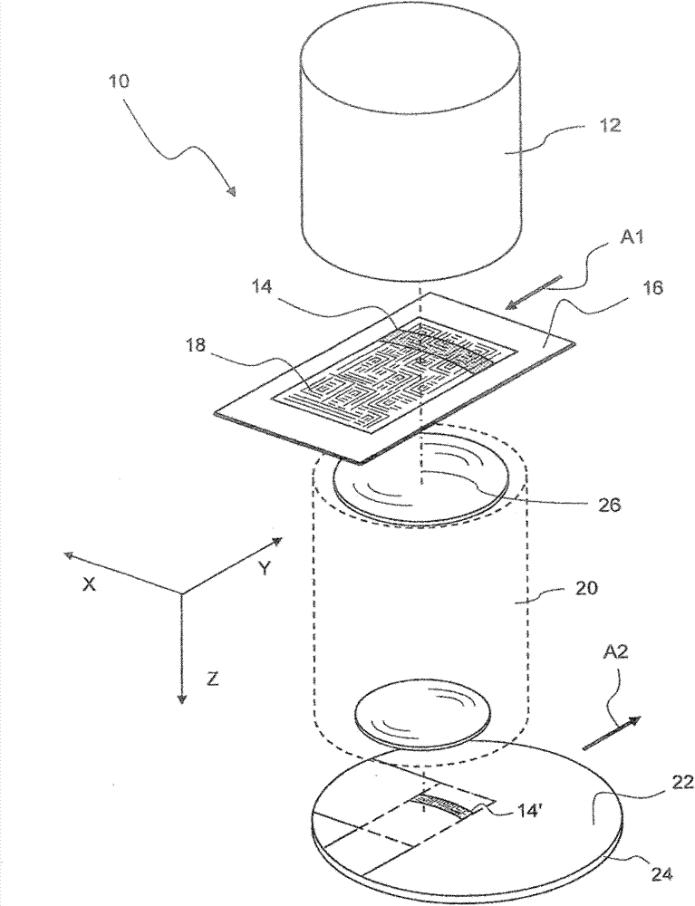
[0054] figure 1 is a perspective and highly simplified view of a projection exposure apparatus 10 comprising an illumination system 12 for generating a projection beam. The projected beam illuminates a field 14 on a mask 16 containing minute structures 18 . In this embodiment, the illuminated field 14 has approximately the shape of a ring segment. However, other (for example rectangular) shaped illumination fields 14 can also be designed, for example.

[0055] The projection objective 20 images the structure 18 within the illuminated field 14 onto a light sensitive layer 22 , such as photoresist, which is deposited on a substrate 24 . Substrate 24 , which may be formed from a silicon wafer, is placed on a wafer stage (not shown) such that the top surface of light-sensitive layer 22 is precisely positioned in the image plane of projection objective 20 . The mask 16 is positioned in the object plane of the projec...


PUM


Abstract

An illumination system of a microlithographic projection exposure apparatus (10) comprises an optical raster element (72) configured to produce a plurality of secondary light sources (95) located in a system pupil surface (70). The optical raster element (72) has a plurality of light entrance facets (92) each being associated with one of the secondary light sources (95). A beam deflecting device comprises a beam deflection array (46) of reflective or transparent beam deflecting elements (M ij ) each being configured to illuminate a spot (90) on one of the light entrance facets (92) at a position that is variable by changing a deflection angle produced by the beam deflecting element (M ij ). A control unit (50) is configured to control the beam deflection elements (M ij ) such that variable light patterns (LP) assembled from the spots (80) can be formed on at least one of the plurality of light entrance facets (92).

Description

technical field [0001] The present invention relates generally to illumination systems for illuminating masks in microlithographic exposure apparatus, and in particular to such systems comprising arrays of mirrors or other beam deflecting elements. The invention also relates to methods of operating such systems. Background technique [0002] Microlithography (also known as photolithography) is a technique used to fabricate integrated circuits, liquid crystal displays, and other microstructured devices. Microlithography processes are used together with etching processes to pattern features in thin film stacks that have been formed on a substrate such as a silicon wafer. In fabricating each layer, the wafer is first coated with photoresist, a material that is sensitive to radiation such as deep ultraviolet (DUV). Next, the wafer with the photoresist on top is exposed to projection light in a projection exposure apparatus. The apparatus projects a mask containing a pattern o...

Claims


Application Information

Patent Timeline
Patent Type & Authority Patents(China)
IPC IPC(8): G03F7/20G02B19/00
CPCG02B26/02G03F7/702G03F7/70066G02B26/101G03F7/70075G03F7/70116G03F7/70158G03F7/70141G02B26/0833G02B19/00G03F7/20
Inventor 马库斯·德冈瑟
Owner CARL ZEISS SMT GMBH
Why Eureka
Try Eureka