Preparation method of field effect transistor

A field-effect transistor and bulk substrate technology, applied in transistors, semiconductor/solid-state device manufacturing, semiconductor devices, etc., can solve the problems of poor miniaturization capability, complex process and high cost, and achieve the effect of reducing the impact

Inactive Publication Date: 2011-06-22
FUDAN UNIV
View PDF2 Cites 6 Cited by
  • Summary
  • Abstract
  • Description
  • Claims
  • Application Information

AI Technical Summary

Problems solved by technology

Its characteristic is that the high-K gate dielectric/metal gate electrode is formed after the impurity activation in the source and drain regions, which eliminates the impact of high-tempera...

Method used


Image

  • Preparation method of field effect transistor
  • Preparation method of field effect transistor
  • Preparation method of field effect transistor

Examples


Embodiment Construction

[0035] Specific embodiments of the present invention will be described in detail below in conjunction with the accompanying drawings.

[0036] The preparation method of the field effect transistor of the present invention can be applied to N-type transistors and P-type transistors, the difference between the two is that the type of doping of the substrate and the source and drain regions is exchanged, that is, the substrate of the N-type transistor is doped with P Type impurities, P-type transistor substrate doped with N-type impurities.

[0037] Please refer to Figure 1-6 , taking the N-type field effect transistor as an example, the preparation method of the field effect transistor of the present invention comprises the following steps:

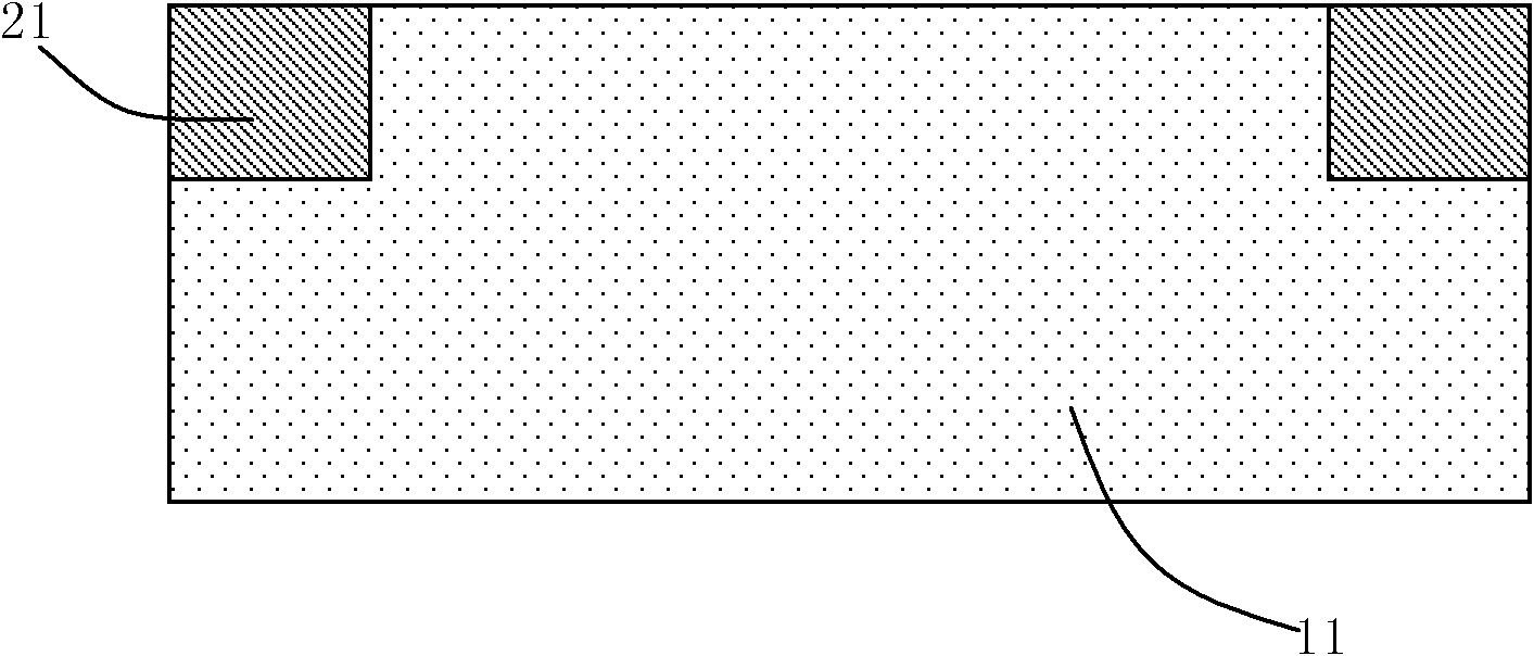
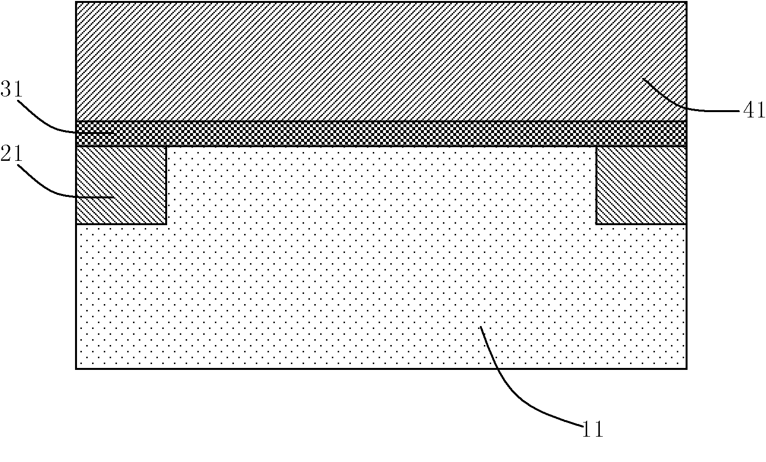
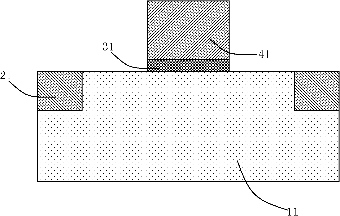
[0038] (1) Provide a P-type bulk silicon substrate 11, use photolithography and etching methods to form shallow trenches, and grow silicon dioxide in the shallow trenches to form shallow trench isolation structures 21 (Shallow TrenchIsola...


PUM


Abstract

The invention provides a preparation method of a field effect transistor, comprising the following steps of: supplying a first molded body substrate, forming a shallow groove by utilizing a photoetching and etching method, and growing to form a silicon dioxide shallow groove isolation structure in the shallow groove; depositing on the first molded body substrate and the silicon dioxide shallow groove isolation structure to form a high-K gate dielectric layer and a metal gate electrode layer; forming a grid electrode structure by utilizing a photoetching or corrosion process and the like; implanting second molded body foreign ions to form a source drain extension area; depositing an insulating layer to form a side wall attached to the edge of a grid electrode; implanting the second molded body foreign ions to form a source drain area of a second molded body field effect transistor and a PN (Performance Number) junction interface positioned between the source drain area and a silicon substrate; and carrying out microwave annealing to activate the implanted ions. The novel process of the field effect transistor can activate the impurities in the source drain area at lower temperature and reduce the influence of source drain annealing on a high-K gate dielectric/metal gate electrode.

Description

【Technical field】 [0001] The invention relates to a semiconductor manufacturing method, in particular to a field effect transistor manufacturing method. 【Background technique】 [0002] With the development of semiconductor technology, metal-oxide-semiconductor field effect transistors (MOSFETs) have been widely used. In recent years, microelectronics technology with silicon integrated circuits as the core has developed rapidly. The development of integrated circuit chips basically follows Moore's law, that is, the integration level of semiconductor chips doubles every 18 months. [0003] However, with the continuous increase in the integration of semiconductor chips, the channel length of the MOSFET is also continuously shortened. When the channel length of the MOSFET becomes very short, serious short-channel effects will occur, such as: the channel length decreases After reaching a certain level, the proportion of the depletion region of the source and drain junctions in t...

Claims


Application Information

Patent Timeline
IPC IPC(8): H01L21/336H01L21/324
CPCH01L21/324H01L29/66477H01L29/517H01L29/6659H01L21/26513H01L21/2658
Inventor 吴东平朴颖华朱志炜张世理张卫
Owner FUDAN UNIV
Why Eureka
Try Eureka