Semiconductor plastic-sealed body and layered scanning method

A layered scanning, semiconductor technology, applied in semiconductor devices, semiconductor/solid-state device manufacturing, semiconductor/solid-state device components, etc., can solve the problems of slow grinding speed, slow speed, incompatibility, etc., to avoid the effect of slow speed

Active Publication Date: 2011-06-22
NANTONG FUJITSU MICROELECTRONICS
View PDF10 Cites 6 Cited by
  • Summary
  • Abstract
  • Description
  • Claims
  • Application Information

AI Technical Summary

Problems solved by technology

[0005] 1. Due to the manual grinding, it cannot be polished in batches, so the grinding speed is slow, and it takes up a lot of human resources and the cost is high;
[0006] 2. The consistency is poor, manual grinding is used, and the grinding degree of each product is different, so when detecting delamination, only one by one scanning can be performed, which is also one of the reasons for the slow speed and high cost
[0007] 3. The accuracy is poor, because during the grinding process, the stress itself generated on the surface of the product, especially the surface of the thinner product, will cause micro-cracks to appear between the molding compound and the lead frame, resulting in misjudgment of the delamination phenomenon
[0008] Therefore, the traditional method is only suitable for use in individual experiments or evaluations, and is not suitable for use in daily monitoring under mass production conditions.

Method used


Image

  • Semiconductor plastic-sealed body and layered scanning method
  • Semiconductor plastic-sealed body and layered scanning method
  • Semiconductor plastic-sealed body and layered scanning method

Examples


Embodiment Construction

[0025] The present invention will be further described below in conjunction with the accompanying drawings and specific embodiments.

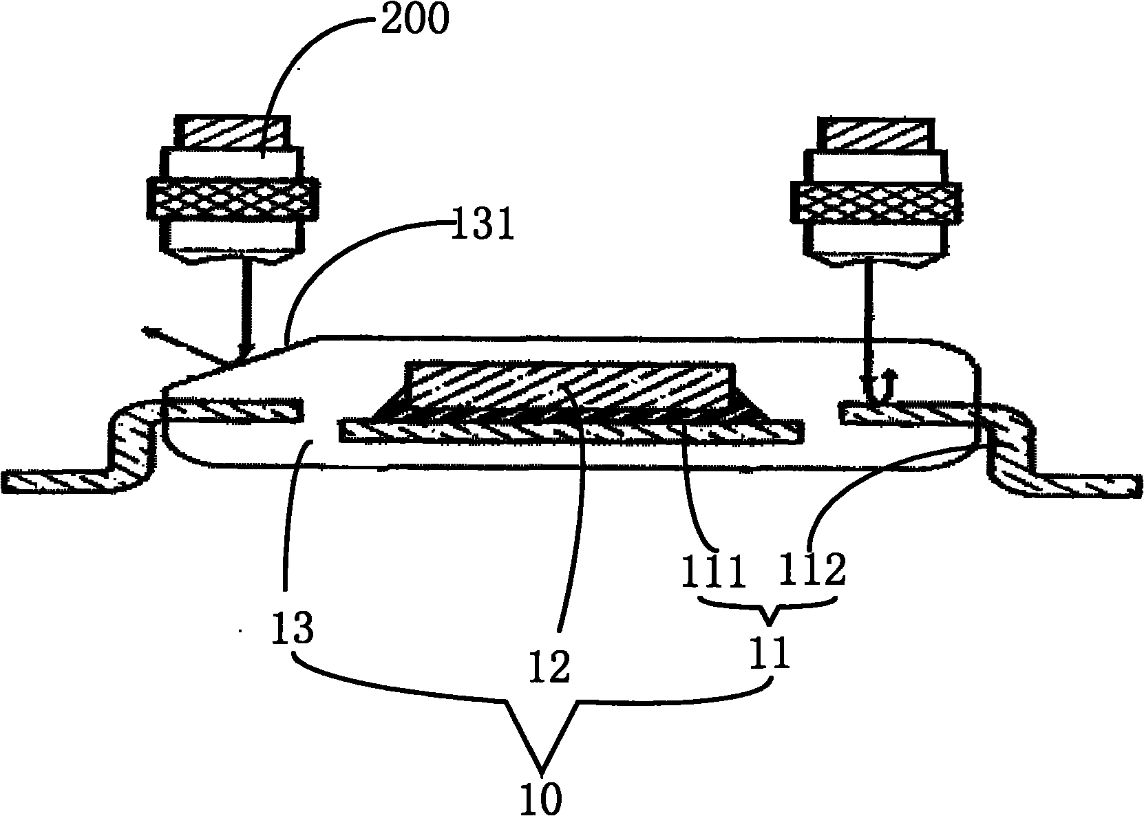
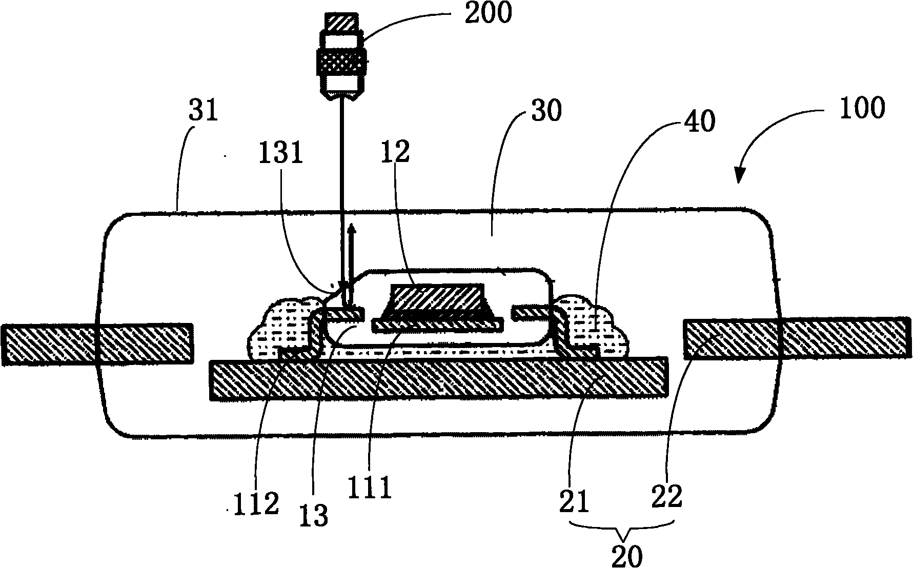
[0026] Please refer to figure 2 , the layered scanning method of the present invention is used for figure 1 The semiconductor plastic packaged device 10 to be inspected is scanned in layers to detect the layering of the interface between different media inside the semiconductor device 10 .

[0027] The semiconductor device 10 includes an inner lead frame 11, a chip 12 fixed on the inner lead frame 11 and an inner plastic package 13 that encapsulates the inner lead frame 11 and the chip 12, the inner lead The frame 11 has a carrier table 111 for fixing the chip 12 and a plurality of pins 112 protruding from the inner plastic package 13 , and the surface of the inner plastic package 13 is formed with a slope 131 .

[0028] The layered scanning method of the present invention utilizes at least one scanner 200 to scan the semiconductor device 10...


PUM


Abstract

The invention relates to a layered scanning method, which comprises the following steps of: coating a lead frame with high temperature-resistance glue; placing a semiconductor device on the lead frame; baking and curing the lead frame; re-packaging the semiconductor device to fill an inclined plane of the semiconductor device into a scanning plane and form an external plastic-sealed body in whichat least the semiconductor is packaged; and scanning an interface of different media inside the semiconductor device by using ultrasonic waves which are perpendicular to the scanning plane and emitted from a scanner. The invention also provides a semiconductor plastic-sealed body. In the invention, changes on the direction of a reflected wave are avoided through the steps of re-packaging a product to be detected and filling the inclined plane on the surface of the plastic-sealed body into the plane; and the invention has the characteristics of high speed, consistency and scanning accuracy andis suitable for daily inspection under the condition of mass production.

Description

technical field [0001] The invention relates to an internal failure analysis method of a semiconductor product, in particular to a semiconductor packaging structure and a layered scanning method thereof. Background technique [0002] Due to the different expansion coefficients of lead frames, plastic packaging materials, chips and other media in semiconductor plastic packages, microcracks or gaps may appear at the interface of different media due to thermal expansion and contraction, that is, delamination. This kind of microcracks or gaps It will cause the product to fail during use, and in severe cases, the phenomenon of "popcorn" will appear and the product will be scrapped. Moreover, since the low-cost requirement of semiconductor packaging is becoming more and more intense, the continuous use of some low-cost materials in the packaging process leads to an increase in the probability of delamination. [0003] Please refer to figure 1 , in order to monitor the quality of...

Claims


Application Information

Patent Timeline
IPC IPC(8): H01L23/31G01N29/04H01L21/56
CPCH01L2224/32245H01L2924/181
Inventor 石海忠赵亚俊吉加安尹华苏红娟
Owner NANTONG FUJITSU MICROELECTRONICS
Why Eureka
Try Eureka