3D semiconductor device
A semiconductor, three-dimensional technology, applied in the field of three-dimensional semiconductor devices, can solve problems such as the limitation of integration of two-dimensional semiconductor memory, and achieve the effect of low manufacturing cost
- Summary
- Abstract
- Description
- Claims
- Application Information
AI Technical Summary
Problems solved by technology
Method used
Image

Examples
no. 1 approach
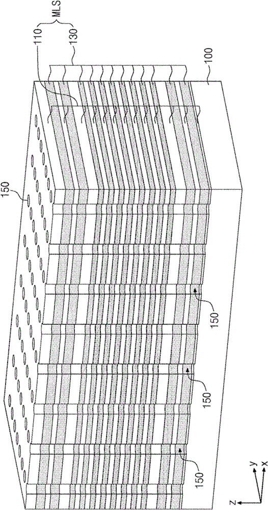
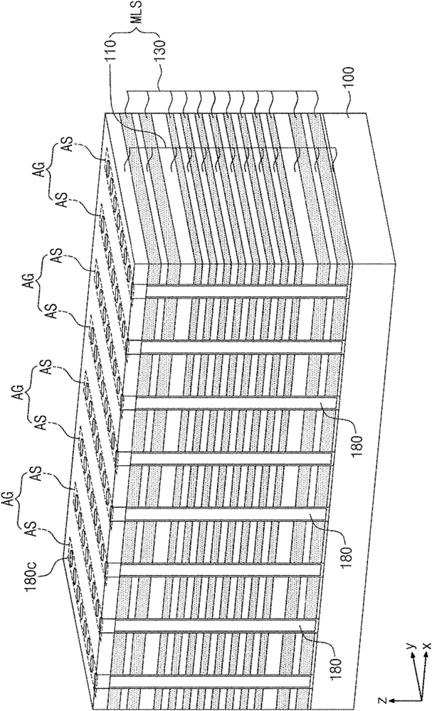
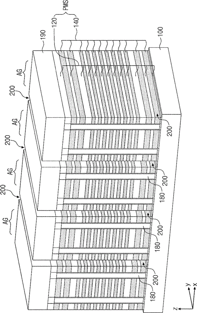
[0038] Figure 1 to Figure 5 is a perspective view illustrating a method of manufacturing a three-dimensional semiconductor device according to a first embodiment of the inventive concept. Figure 6 to Figure 8 is a perspective view showing a part of the three-dimensional semiconductor device according to the first embodiment of the inventive concept in more detail.
[0039] refer to figure 1, the molding layer structure MLS is formed on the substrate 100 and then patterned to form the active opening 150 for exposing the upper surface of the substrate 100 .
[0040] For example, the substrate 100 may be formed of a semiconductor material (eg, a silicon wafer), an insulating material (eg, glass), and one of a semiconductor member or a conductive member covered with an insulating film. The substrate 100 may have an upper surface parallel to the xy plane. The active opening 150 may be two-dimensionally formed on the substrate 100 or an xy plane.
[0041] The molding layer str...
no. 2 approach
[0069] Figure 10 to Figure 12 , Figure 13A , Figure 14A and Figure 15A is a perspective view illustrating a method of manufacturing a three-dimensional semiconductor device according to a second embodiment of the inventive concept. Figure 13B , Figure 14B to Figure 14D as well as Figure 15B to Figure 15D It is a perspective view that provides the technical spirit for understanding the inventive concept. Particularly, Figure 10 to Figure 12 as well as Figure 13A to Figure 15A is a perspective view showing a method of manufacturing a semiconductor device according to an embodiment in a predetermined first viewing angle. Figure 13B to Figure 15B is a perspective view showing that in a second viewing angle different from the first viewing angle Figure 13A , Figure 14A and Figure 15A semiconductor device shown in . Figure 14C and Figure 14D is the perspective view used to explain in more detail the Figure 14A The technical characteristics described in. ...
PUM
 Abstract
Description
Claims
Application Information
 - R&D
- Intellectual Property
- Life Sciences
- Materials
- Tech Scout
- Unparalleled Data Quality
- Higher Quality Content
- 60% Fewer Hallucinations
Browse by: Latest US Patents, China's latest patents, Technical Efficacy Thesaurus, Application Domain, Technology Topic, Popular Technical Reports.
© 2025 PatSnap. All rights reserved.Legal|Privacy policy|Modern Slavery Act Transparency Statement|Sitemap|About US| Contact US: help@patsnap.com