
Semiconductor device

A semiconductor and device technology, applied in the field of high-k gate dielectric CMOS devices, can solve the problems of carrier mobility degradation, degradation, high interface state, etc., and achieve the effect of improving electron mobility, improving overall performance and reducing EOT

Active Publication Date: 2011-06-22
INST OF MICROELECTRONICS CHINESE ACAD OF SCI
View PDF0 Cites 25 Cited by
  • Summary
  • Abstract
  • Description
  • Claims
  • Application Information

AI Technical Summary

Problems solved by technology

The resulting problem is that with the continuous thinning of the interface layer, some atoms in the high-k gate dielectric material will diffuse to the channel region of the semiconductor substrate through the ultra-thin interface layer under high-temperature heat treatment. In turn, the carrier mobility of the channel region is degraded, and the problem of carrier mobility degradation caused by atomic diffusion in the high-k gate dielectric is more serious for NMOS devices, and the impact is relatively serious for PMOS devices much smaller
Moreover, SiON with a large dielectric constant is commonly used in the interface layer in the prior art. x , but the resulting problem is that the introduction of N in the interface layer will degrade the carrier mobility, especially the electron carrier mobility of NMOS devices
In addition, when the high-k gate dielectric is in direct contact with the semiconductor substrate, a higher interface state will be generated, which will also degrade the carrier mobility, especially the electron carrier mobility, which will affect the carrier mobility of the NMOS device. rate has a big impact on

Method used


Image

  • Semiconductor device
  • Semiconductor device
  • Semiconductor device

Examples


no. 1 example

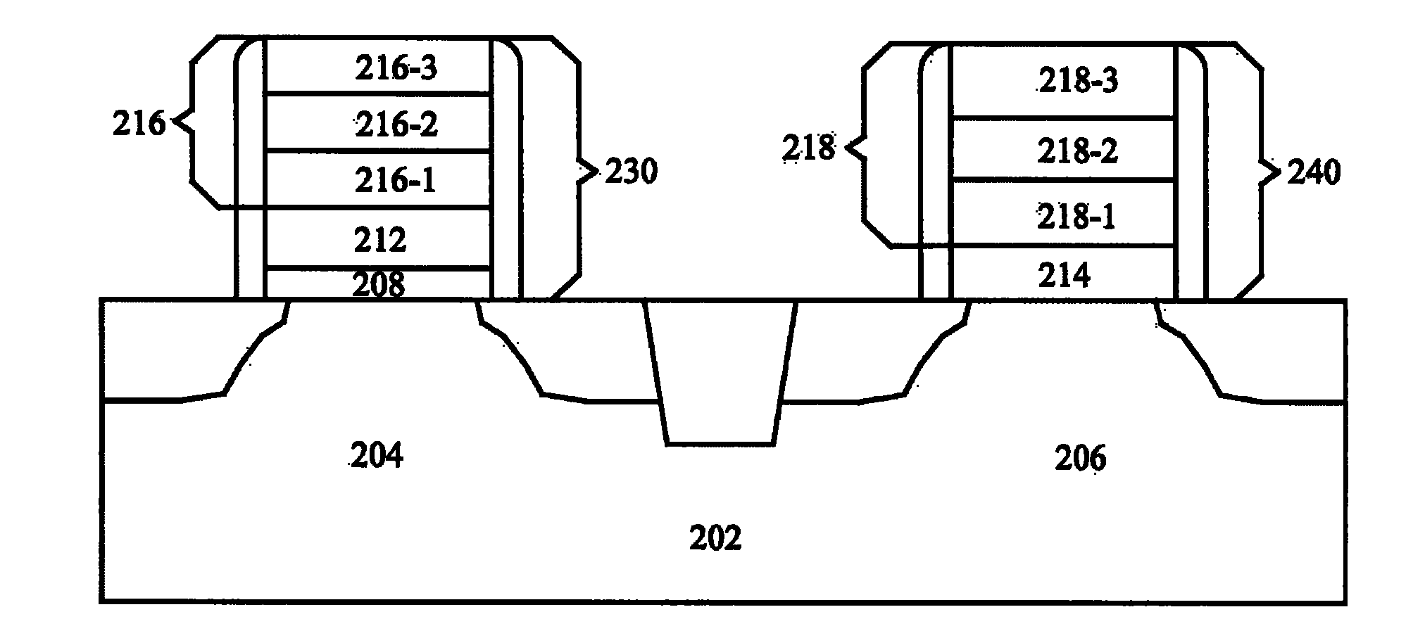
[0014] refer to figure 1 , figure 1 A schematic structural diagram of a semiconductor device according to an embodiment of the present invention is shown. like figure 1 As shown, the device includes: a semiconductor substrate 202 having an NMOS region 204 and a PMOS region 206, the NMOS region 204 is isolated from the PMOS region 206; the semiconductor substrate 202 formed on the NMOS region 204 The first gate stack 230 and the second gate stack 240 formed on the semiconductor substrate 202 of the PMOS region 206, the first gate stack 230 includes: a first interface layer 208; formed on the first interface layer 208 The first high-k gate dielectric layer 212 on the first high-k gate dielectric layer; the first gate layer 216 formed on the first high-k gate dielectric layer, wherein the first gate layer 216 is one or more layers; the first The second gate stack 240 includes: a second high-k gate dielectric layer 214; a second gate layer 218 formed on the second high-k gate d...

no. 2 example

[0024] A second embodiment of the present invention will be described below. In the second embodiment, different interfacial layers are provided for the NMOS device and the PMOS device, so as to adjust the carrier mobility of the NMOS device and the PMOS device respectively.

[0025] refer to Figure 10 , Figure 10 A schematic structural diagram of a semiconductor device according to a second embodiment of the present invention is shown. like Figure 10 As shown, the device includes: a semiconductor substrate 202 having an NMOS region 204 and a PMOS region 206, the NMOS region 204 is isolated from the PMOS region 206; the semiconductor substrate 202 formed on the NMOS region 204 The first gate stack 230 and the second gate stack 240 formed on the semiconductor substrate 202 of the PMOS region 206; wherein the first gate stack 230 includes: a first interface layer 208; formed on the first interface layer The first high-k gate dielectric layer 212 on 208; the first gate lay...


PUM


Abstract

The invention relates to a semiconductor device, in particular to an interface optimized high-k gate dielectric complementary metal oxide semiconductor (CMOS) device. Interface layers with different thicknesses and different materials are adopted on a semiconductor substrate in an N-channel metal oxide semiconductor (NMOS) region and a semiconductor substrate of a P-channel metal oxide semiconductor (PMOS) region, the equivalent oxide thickness (EOT) of a device, in particular the EOT of a PMOS device, is effectively reduced, and the electron mobility of the device, in particular the electronmobility of an NMOS device is improved, so that the overall performance of the device is effectively improved.

Description

technical field [0001] The invention relates to a semiconductor device, in particular to a high-k gate dielectric CMOS device with optimized interface. Background technique [0002] With the development of semiconductor technology, integrated circuits with higher performance and stronger functions require greater component density, and the size, size and space of each component, between components or each component itself also need to be further reduced. The application of the core technology of 32 / 22 nanometer process integrated circuits has become an inevitable trend in the development of integrated circuits, and it is also one of the topics that major international semiconductor companies and research organizations are competing to research and develop. The gate engineering research of CMOS devices with "high-k / metal gate" technology as the core is the most representative core process in 32 / 22 nanometer technology, and the related material, process and structure research ...

Claims


Application Information

Patent Timeline
Patent Type & Authority Applications(China)
IPC IPC(8): H01L27/092H01L29/43H01L21/283
CPCH01L21/823842H01L21/823462H01L29/517H01L21/82345H01L29/4966H01L21/823857H01L29/513H01L21/28202
Inventor 王文武陈世杰韩锴王晓磊陈大鹏
Owner INST OF MICROELECTRONICS CHINESE ACAD OF SCI
Learn More