Check patentability & draft patents in minutes with Patsnap Eureka AI!

Low voltage differential signaling (LVDS) interface circuit based on field programmable gate array (FPGA) and data transmission method

An interface circuit and data technology, applied in the direction of logic circuit connection/interface layout, etc., can solve the problems between difficult efficiency and training time, maintain balance, complex clock design scheme, etc., achieve high transmission rate, simplify PCB design, save effect of numbers

Inactive Publication Date: 2011-06-22
ALCATEL LUCENT SHANGHAI BELL CO LTD
View PDF2 Cites 13 Cited by
  • Summary
  • Abstract
  • Description
  • Claims
  • Application Information

AI Technical Summary

Problems solved by technology

[0015] As can be seen from the above analysis, it is difficult to maintain a balance between efficiency and training time
[0016] Another problem existing in the prior art is that the design scheme of the clock is very complicated

Method used


Image

  • Low voltage differential signaling (LVDS) interface circuit based on field programmable gate array (FPGA) and data transmission method
  • Low voltage differential signaling (LVDS) interface circuit based on field programmable gate array (FPGA) and data transmission method
  • Low voltage differential signaling (LVDS) interface circuit based on field programmable gate array (FPGA) and data transmission method

Examples


Embodiment Construction

[0029] In the following, the principle and implementation of the present invention will become apparent by describing specific embodiments of the present invention in conjunction with the accompanying drawings. It should be noted that the present invention should not be limited to the specific examples described below.

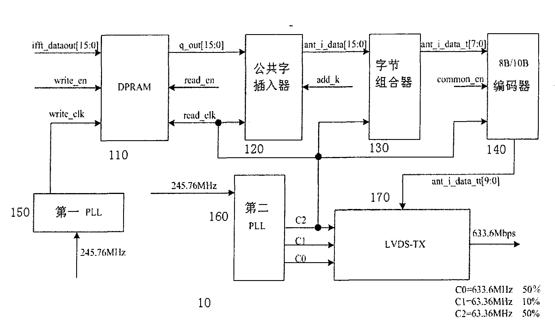
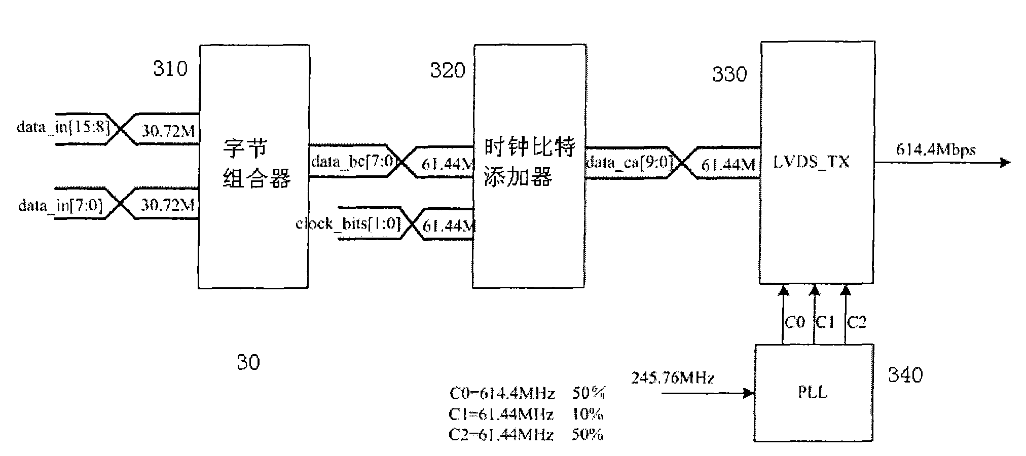
[0030] image 3 is a block diagram showing an FPGA-based LVDS interface circuit for converting parallel data into serial data according to one embodiment of the present invention. Such as image 3 As shown, LVDS interface circuit 30 includes byte combiner 310 , clock bit adder 320 , LVDS-TX interface 330 and PLL 340 . The byte combiner 310 converts multiple channels of low-speed parallel data into one channel of high-speed parallel data for subsequent processing. For illustration, take two-way parallel data as an example. Such as image 3As shown, the byte combiner combines two channels of 8-bit data with a frequency of 30.72MHz into one channel of 8-bit ...


PUM


Abstract

The invention provides a low voltage differential signaling (LVDS) transmission interface circuit based on a field programmable gate array (FPGA), comprising a byte combiner, a clock bit adder, an LVDS transmission interface and a phase locked loop, wherein the byte combiner is used for converting input multi-channel low-speed parallel data into one-channel high-speed parallel data as output; the clock bit adder is used for adding clock bits to the one-channel high-speed parallel data; the LVDS transmission interface is used for converting the parallel data to which the clock bits are added into serial data for transmission; and the phase locked loop is used for providing clock signals for the LVDS transmission interface. The invention also provides an LVDS transmission method. According to the invention, the high-speed data can be received efficiently and stably, the training time is shortened, and the design scheme of a clock is simplified.

Description

technical field [0001] The invention relates to the field of digital circuits, in particular to an FPGA-based LVDS interface circuit and a data transmission method. Background technique [0002] LVDS (Low Voltage Differential Signaling) is a serial-parallel / parallel-serial conversion interface for data transmission between chips. At the sending end, multiple channels of parallel data are combined into one channel for transmission, while at the receiving end, one channel of data is converted into multiple channels for reception. In the prior art, due to the high speed serial data stream, the skew of the transmitted data, and the added skew of the link, it is difficult for the receiver to establish the correct receive word boundary and rearrange the data. [0003] The usual method is that the LVDS interface circuit must insert common words in the data stream and encode them according to 8B / 10B. 8B / 10B is also called 8 bytes / 10 bytes or 8B10B. Specifically, 8B / 10B encoding i...

Claims


Application Information

Patent Timeline
Patent Type & Authority Applications(China)
IPC IPC(8): H03K19/0175
Inventor 李优杏何虎刚
Owner ALCATEL LUCENT SHANGHAI BELL CO LTD
Features
  • R&D
  • Intellectual Property
  • Life Sciences
  • Materials
  • Tech Scout
  • Unparalleled Data Quality
  • Higher Quality Content
  • 60% Fewer Hallucinations
Learn More