
Optical transmitter and receiver apparatus

A technology of optical transceiver and optical fiber, which is applied in the field of optical transceiver devices, can solve the problems of high price, 45° reflector takes a lot of time and cost, and high power consumption, and achieves the effects of low power consumption, low heat generation, and improved installation strength

Inactive Publication Date: 2011-06-29
THE FUJIKURA CABLE WORKS LTD
View PDF13 Cites 3 Cited by
  • Summary
  • Abstract
  • Description
  • Claims
  • Application Information

AI Technical Summary

Problems solved by technology

However, there is such a problem in this method that it takes a lot of time and cost to form the 45° mirror
Also, since VCSELs are not used, power consumption is high and the price is high

Method used


Image

  • Optical transmitter and receiver apparatus
  • Optical transmitter and receiver apparatus
  • Optical transmitter and receiver apparatus

Examples


Embodiment 1

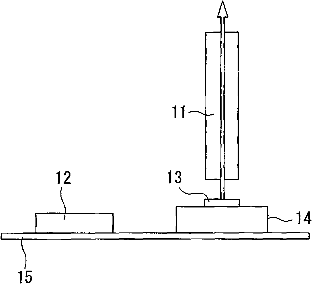
[0109] make Figure 4 The sub-mounted substrate shown. The material of the submount substrate is aluminum nitride. The electrode material on the sub-mount substrate is made of gold-tin alloy in consideration of the connection strength with the gold wire when mounting the light-receiving and light-emitting elements.

[0110] Such as Figure 4 As shown in , mount the light-receiving and emitting elements on the sub-mount substrate. The mounting is done with conductive silver paste and gold wires. The light-emitting element uses a VCSEL with an emission center wavelength of 850nm, and the light-receiving element uses a PD.

[0111] Next, the sub-mount substrate on which the light-receiving and light-emitting elements are mounted on the side is mounted on the printed circuit board. The submount substrate is transported by vacuum tweezers, and soldered to the electrode pads of the printed circuit board with conductive silver paste.

[0112] Next, alignment and fixation of the...

Embodiment 2

[0116] Using the optical communication module actually manufactured according to the manufacturing method of the present invention, an image transmission experiment was carried out.

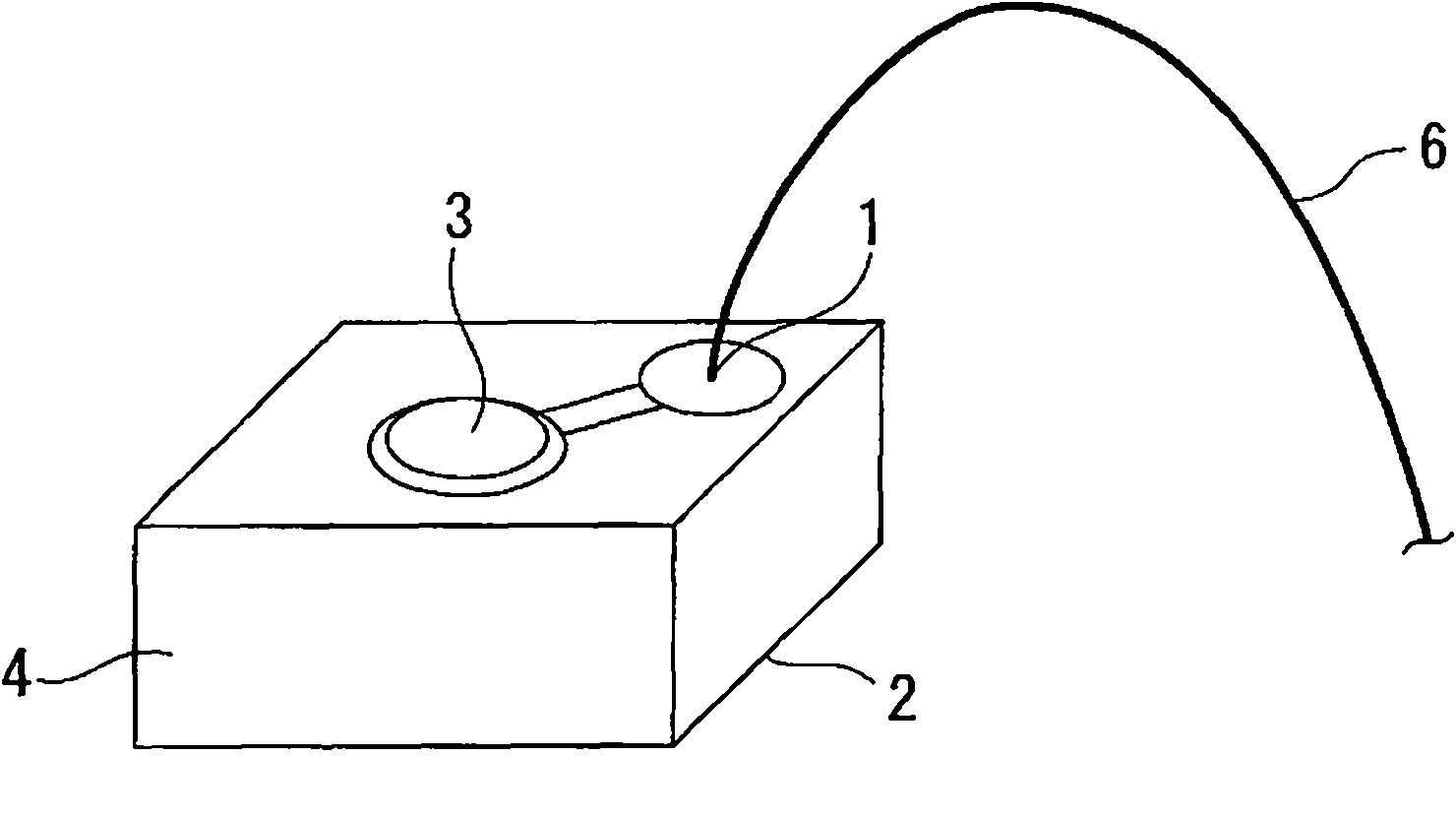
[0117] As a light emitting element, a surface emitting laser (VCSEL) with an emission wavelength of 850 nm and a cutoff frequency of 2.5 GHz was used. VCSEL uses commercially available products such as figure 1 As shown, the selected type is an element of the type in which the anode is bonded to the electrode using wire bonding and the cathode is bonded to the electrode using conductive paste.

[0118] As a light receiving element, a GaAs photodiode (PD) with a cutoff frequency of 2.5 GHz was used. For the PD, a commercially available product is used, and the shape is selected to be an element in which the anode is conductive by wire bonding and the cathode is conductive by conductive paste, similarly to the VCSEL.

[0119] As the submount substrate, the same substrate as the submount substrate...

Embodiment 3

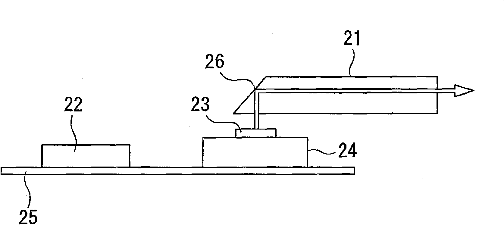
[0132] An optical transceiving device is used between the head-mounted display 123 and its control device 125 . A brief composition is shown in Figure 15 . This device is a goggle-type head-mounted display 123 worn on the head by the subject 124, and is in a form matched and fixed to the outer circumference of one ear, and the optical waveguide 126 is taken out from the rear of the part worn on the ear. In order to improve the matching feeling to the ear, and for the sake of designability, the extraction part of the optical waveguide 126 is as follows: Figure 16 As shown, it includes: a printed circuit board 127 disposed on the rear end of the head-mounted display 123, a sub-mounted substrate 128 mounted on the printed circuit board 127, a light-receiving and light-emitting element mounted on the side of the sub-mounted substrate 128, and a light-emitting diode. The optical waveguide path 129 connected to the element by coupling. Since the head-mounted display 123 is smal...


PUM

PropertyMeasurementUnit
diameteraaaaaaaaaa
refractive indexaaaaaaaaaa

Abstract

The invention provides an optical transmitter and receiver apparatus including: a printing substrate; a sub-mount substrate formed by mounting one or both of a light-emitting element and a light-receiving element on a side surface; and an optical waveguide aligned between the light-emitting element and light-receiving element and can be optically coupled with elements. The light-emitting element and light-receiving element possess front surfaces for emitting or receiving light, back surfaces connected with the sub-mount substrate, and the light-emitting and -receiving directions of the light-emitting element and light-receiving element are perpendicular to the sub-mount substrate. The light-emitting element and light-receiving element are arranged on the printed substrate in the form thatthe light-emitting and -receiving directions of the light-emitting element and light-receiving element are not perpendicular to the printed substrate by means of the sub-mount substrate. In addition,the whole sub-mount substrate, the light-emitting element, the light-receiving element, and the optical waveguide end adjacent to the light elements are all covered with resin.

Description

[0001] This application is a divisional application for the application dated February 22, 2008, the application number is 200880015472.7, and the invention name is "optical communication module and its manufacturing method and optical transceiver". technical field [0002] The present invention relates to an optical communication module formed by coupling a light-emitting element, a light-receiving element, and an optical waveguide path, a manufacturing method thereof, and an optical transceiver. [0003] This application claims the priority of Japanese Patent Application No. 2007-127810 for which it applied to Japan on May 14, 2007, and uses the content here. Background technique [0004] The optical communication module has been expected to be small and inexpensive. As a light emitting element used in this optical communication module, a VCSEL (surface emitting laser) has been studied in recent years. The bare chip of VCSEL is usually such as figure 1 Shown is a structu...

Claims


Application Information

Patent Timeline
Patent Type & Authority Applications(China)
IPC IPC(8): G02B6/43G02B6/42
CPCG02B6/4202G02B6/43H01S5/02284H01L2224/48091H01L2224/48247H01L2224/45144Y10T29/49826H01S5/02251H01L2924/00014H01L2924/00
Inventor 寺田佳弘大桥正和畔上幸士市井健太郎
Owner THE FUJIKURA CABLE WORKS LTD
Learn More