Testability circuit for digital/analog mixed signal chip

A signal and circuit technology, applied in the field of testable circuits, to achieve the effect of enhancing ESD capability and reducing test pins

Inactive Publication Date: 2011-07-06
SHANGHAI HUAHONG INTEGRATED CIRCUIT
View PDF2 Cites 8 Cited by
  • Summary
  • Abstract
  • Description
  • Claims
  • Application Information

AI Technical Summary

Problems solved by technology

However, for digital-analog mixed-signal circuits, there is currently no EDA tool that can automatically add testability circuits

Method used


Image

  • Testability circuit for digital/analog mixed signal chip
  • Testability circuit for digital/analog mixed signal chip
  • Testability circuit for digital/analog mixed signal chip

Examples


Embodiment Construction

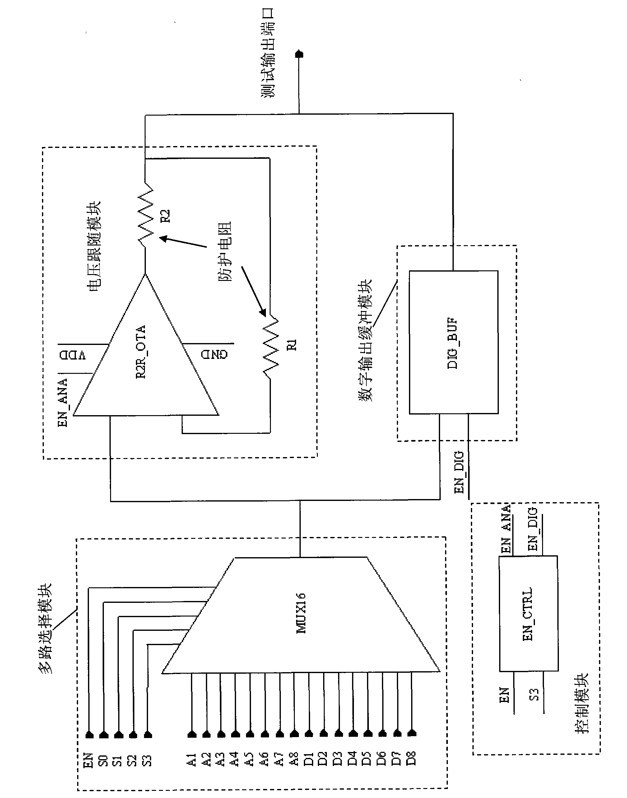
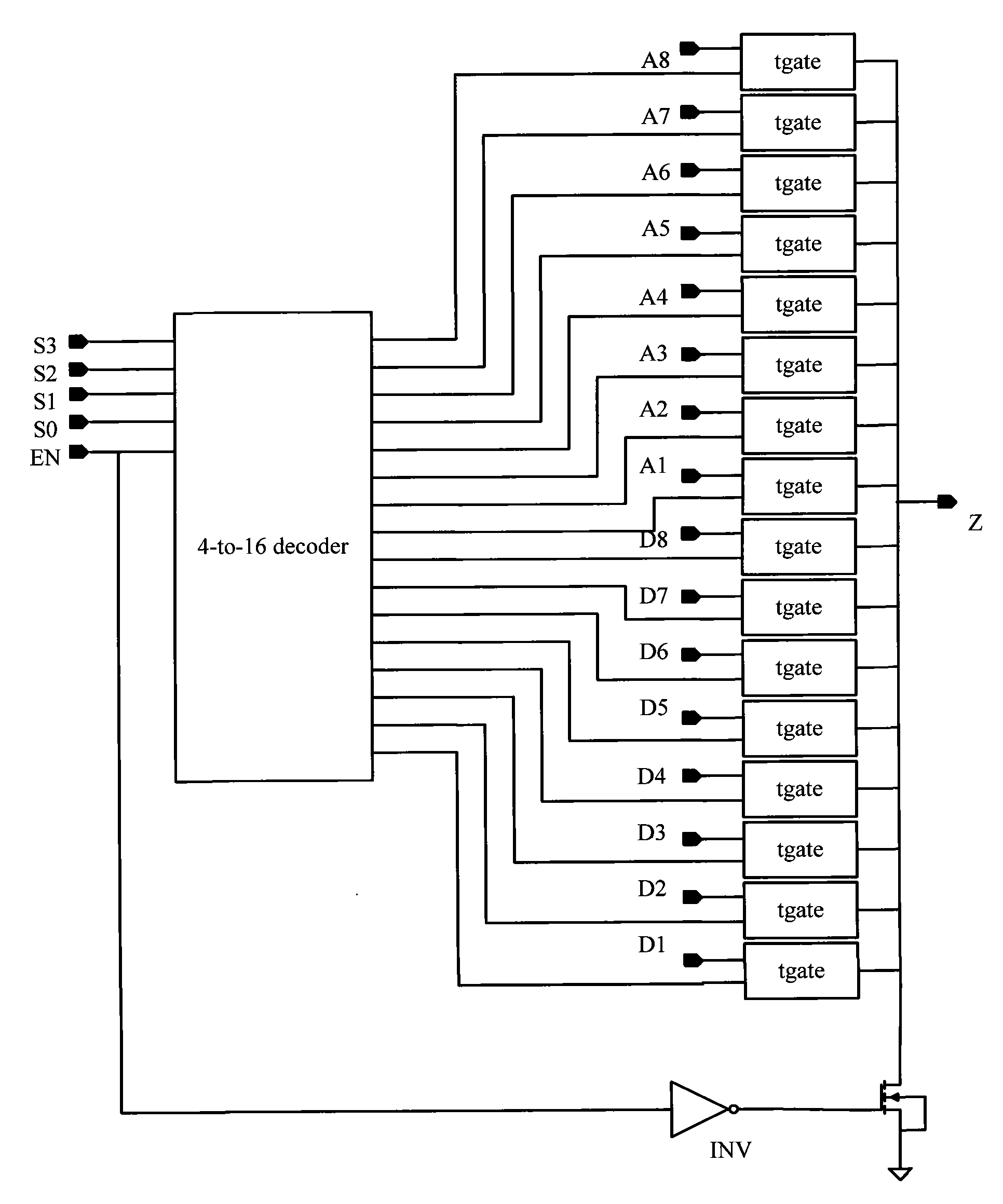
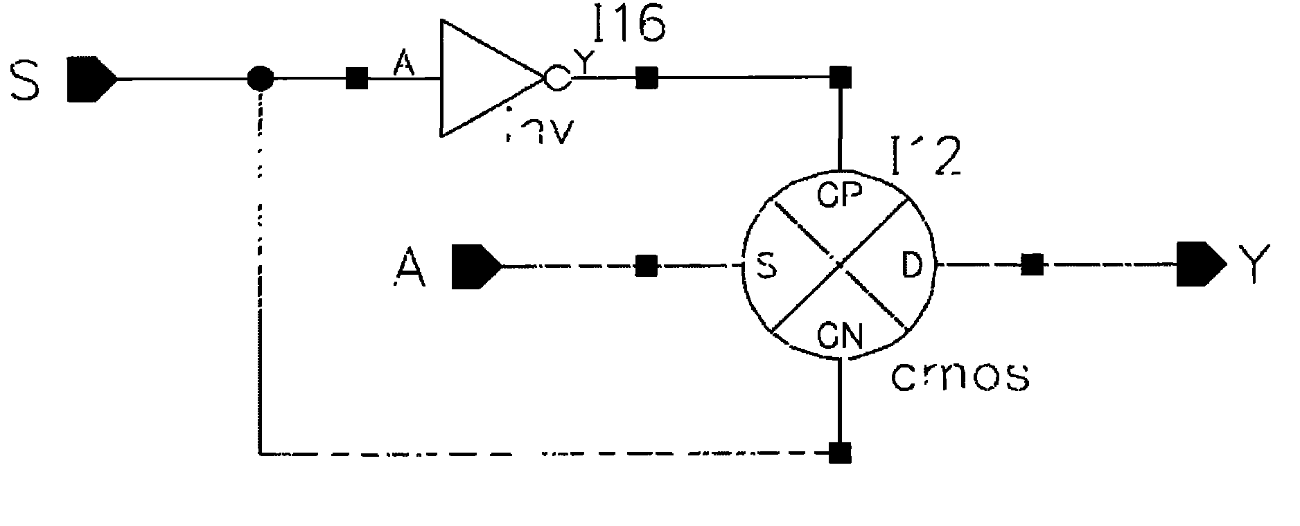
[0023] The testability circuit for the digital-analog mixed-signal chip of the present invention (see figure 1 ), including: a multiplexer module, a control module, a voltage follower module, and a digital output buffer module; the multiplexer module is used to select the signal to be observed according to the enable signal and the selection signal, and send it to the voltage Follower module or digital output buffer module, if it is a digital signal, it will be sent to the digital output buffer module, if it is an analog signal, it will be sent to the voltage follower module; the control module is used to generate control signals according to the enable signal and selection signal , to control whether to turn on the voltage follower module or the digital output buffer module, if it is an analog signal, turn on the voltage follower module, and if it is a digital signal, turn on the digital output buffer module. The control module is a combined logic circuit, which can be formed...


PUM


Abstract

The invention discloses a testability circuit for a digital / analog mixed signal chip. The testability circuit comprises a multi-path selection module, a control module, a voltage follower module and a digital output buffer module, wherein the multi-path selection module is used for selecting the signal to be observed and transmitting the signal to the voltage follower module or the digital output buffer module; the control module is used for generating a control signal to selectively open the voltage follower module or the digital output buffer module; and the selected signal is transmitted to the voltage follower module if the selected signal is an analog signal, or the selected signal is transmitted to the digital output buffer module if the selected signal is a digital signal. The testability circuit can observe the important digital signal and the analog signal in the chip through an output pin of the chip, which facilitates the chip fault analysis and debugging. The testability circuit is suitable for the digital / analog mixed signal chip and full-custom chip.

Description

technical field [0001] The invention relates to a testability circuit for observing digital signals and analog signals in a digital-analog mixed signal chip or a fully customized chip. Background technique [0002] With the development of integrated circuit technology, the scale of integrated circuits is rapidly expanding, and the circuit structure is becoming more and more complex. It is becoming more and more difficult to test chips. The cost of testing is often higher than the cost of design. The cost of testing has become the cost of product development. The length of the test time also directly affects the time to market of the product and thus affects the economic benefits. In order to keep the test cost within a reasonable limit, the most effective method is to adopt design for test (DFT) technology in chip design. Therefore, in the past, the designer designed the circuit according to the demand, and the traditional practice of the tester formulating the test plan ba...

Claims


Application Information

Patent Timeline
Patent Type & Authority Applications(China)
IPC IPC(8): G06F17/50
Inventor 范志祥刘颖
Owner SHANGHAI HUAHONG INTEGRATED CIRCUIT
Why Eureka
Try Eureka