Infrared focal plane detector packaging window and manufacturing method thereof

An infrared focal plane and detector technology, which is applied in semiconductor devices, final product manufacturing, sustainable manufacturing/processing, etc., can solve problems such as easy air leakage of detectors, poor vacuum performance, and reduced packaging yield

Inactive Publication Date: 2011-07-06
上海欧菲尔光电技术有限公司
View PDF5 Cites 6 Cited by
  • Summary
  • Abstract
  • Description
  • Claims
  • Application Information

AI Technical Summary

Problems solved by technology

[0008] 1. The packaging process is complex
[0009] The packaging process requires several steps such as cleaning, gluing, and curing. The process is complicated and reduces ...

Method used


Image

  • Infrared focal plane detector packaging window and manufacturing method thereof
  • Infrared focal plane detector packaging window and manufacturing method thereof
  • Infrared focal plane detector packaging window and manufacturing method thereof

Examples


Embodiment 1

[0045] According to the above-mentioned manufacturing method, a 7.0um cut-off infrared focal plane detector packaging window for thermal imaging cameras was manufactured.

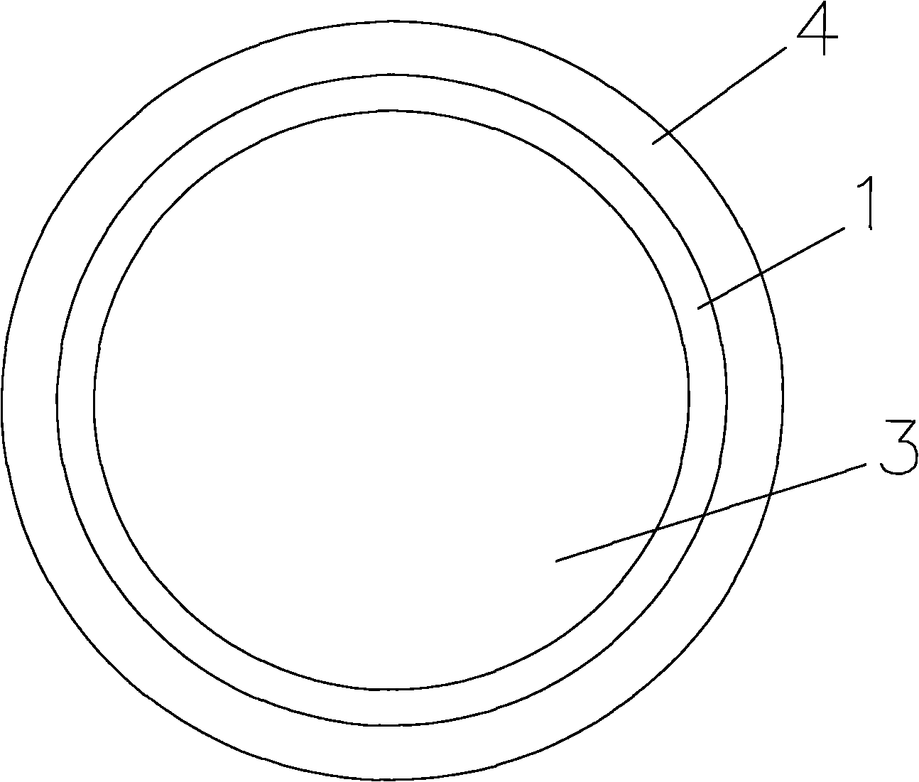
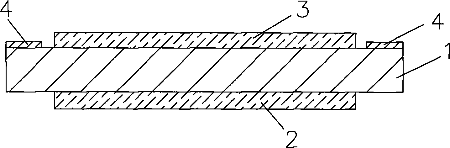
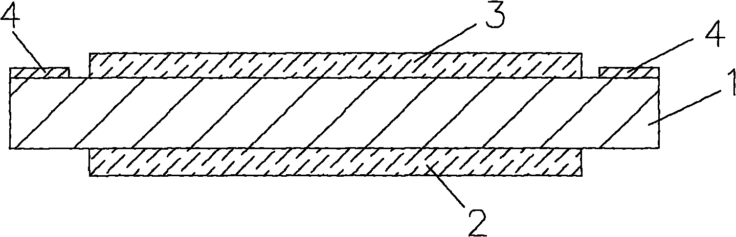
[0046] The substrate material is Si, the infrared thin film material is Ge and ZnS, and the metal welding layer material is Cr, Ni, Au.

[0047] The infrared optical film structure on the back is 1Sm-1.256L-2.951H-2.452L-2.752H2.274L-2.186H-2.407L-2.758H-2.612L-2.867H-2.153L-2.201H-2.693L-3.038H- 2.591L-4.714H-2.66L-3.432H-3.525L-4.319H-2.382L-3.861H-4.085L-3.257H-2.134L-5.305H-6.288L, where Sm represents Si substrate, H represents Ge, L stands for ZnS, and the data are in optical units.

[0048] The front optical film structure is 1Sm-1.198H-0.783L-1.362H-0.796L-1.46H0.859L-0.982H-1.247L-1.003H-1.307L-0.684H-1.128L-1.064H-1.137L-1.237 H-1.307L-1.682H-1.148L-1.815H-1.072L-1.162H-1.84L-1.446H-1.49L-1.261H-1.65L-1.516H-1.257L-1.996H-1.655L-1.901H- 2.084L-2.144H-1.633L-2.195H-1.727L-2.381H-2.36L-1.053H-2.65...

Embodiment 2

[0052] According to the above manufacturing method, a 8.5-12um transparent infrared focal plane detector packaging window is manufactured.

[0053] The substrate material is Ge, the infrared thin film material is PbTe and ZnSe, and the metal welding layer material is Ti, Ni, Au.

[0054]The infrared optical film structure on the back is 1Sm-0.478L-1.041H-0.994L-1.101H-1.006L-1.004H-0.972L-1.342H-0.971L-0.971H-1.011L-1.006H-0.561L-0.811L -1.023H-1.447L-1.732H-1.434L-1.624H-1.577L-1.033H-1.542L-1.81H-1.359L-2.209H-0.983L-1.133L-1.595H-1.818L-2.618H-1.608 L-1.611H-2.375L-2.352H-0.649L-3.551H-3.7L. Among them, Sm represents Ge substrate, H represents PbTe, L represents ZnSe, and the data are in optical units.

[0055] The front optical film structure is 1Sm-1.389H-0.122L-1.393H-1.121L-1.043H-1.051L-1.027H-1.038L-1.023H-1.034L-1.021H-1.032L-1.022H-1.033L- 1.023H-1.035L-1.027H-1.043L-1.04H-1.075L-1.02H-0.518L. Among them, Sm represents Ge substrate, H represents PbTe, L represen...


PUM


Abstract

The invention provides an infrared focal plane detector packaging window and a manufacturing method thereof. The packaging window comprises a substrate, wherein an infrared optical thin film for wavelength cutoff is plated in the middle part of the front side of the substrate; an infrared optical thin film for wavelength cutoff is plated in the middle part of the back side of the substrate; and a metal thin film for packaging is plated on the periphery. The manufacturing method is as follows: the infrared optical thin films and the metal thin film are all plated by using a vacuum thermal evaporation method. The wavelength cutoff function of the packaging window and a vacuum packaging function are integrated, and two functions are simultaneously realized on the same substrate, thereby increasing the packaging yield, and solving the problem of vacuum air leakage of the original packaging window.

Description

technical field [0001] The invention relates to an optical device, in particular to an infrared focal plane detector packaging window and a manufacturing method thereof. Background technique [0002] Infrared focal plane detector is the core component of infrared imaging optical system, widely used in infrared remote sensing, night vision, medical treatment, rescue, military, electric power and other fields. The infrared focal plane detector is composed of a package window, a photoelectric conversion layer, a readout circuit and a package tube shell. The encapsulation window has the following functions: [0003] 1. Wavelength cut-off [0004] The photoelectric conversion layer responds to a wide range of wavelengths, and it is necessary to filter out light waves that do not need to be detected. This function is realized by coating an infrared optical film on the packaging window. [0005] 2. Vacuum packaging [0006] The photoelectric conversion layer needs to be in a va...

Claims


Application Information

Patent Timeline
IPC IPC(8): H01L31/0203H01L31/18
CPCY02P70/50
Inventor 周东平赵培
Owner 上海欧菲尔光电技术有限公司
Why Eureka
Try Eureka