MEMS microphone and encapsulation method thereof

A packaging method and technology for microphones, which are applied to sensors, electrostatic transducers, microphones, electrical components, etc., can solve the problems of non-adhesion and firmness of conductive adhesives, deformation, and complicated manufacturing processes, and are conducive to large-scale production. The effect of promotion, simple bonding process and lower production cost

Active Publication Date: 2011-07-06
WEIFANG GOERTEK MICROELECTRONICS CO LTD
View PDF8 Cites 12 Cited by
  • Summary
  • Abstract
  • Description
  • Claims
  • Application Information

AI Technical Summary

Problems solved by technology

Obviously, the manufacturing process of this structure is relatively complicated, which is not conducive to cost control
[0005] In addition, there are some designs that directly use conductive adhesive to fix and bond the shell and the circuit board together, but the conductive adhesive generally does not have too strong adhesion and firmness, resulting in insuffici

Method used


Image

  • MEMS microphone and encapsulation method thereof
  • MEMS microphone and encapsulation method thereof
  • MEMS microphone and encapsulation method thereof

Examples


no. 1 example

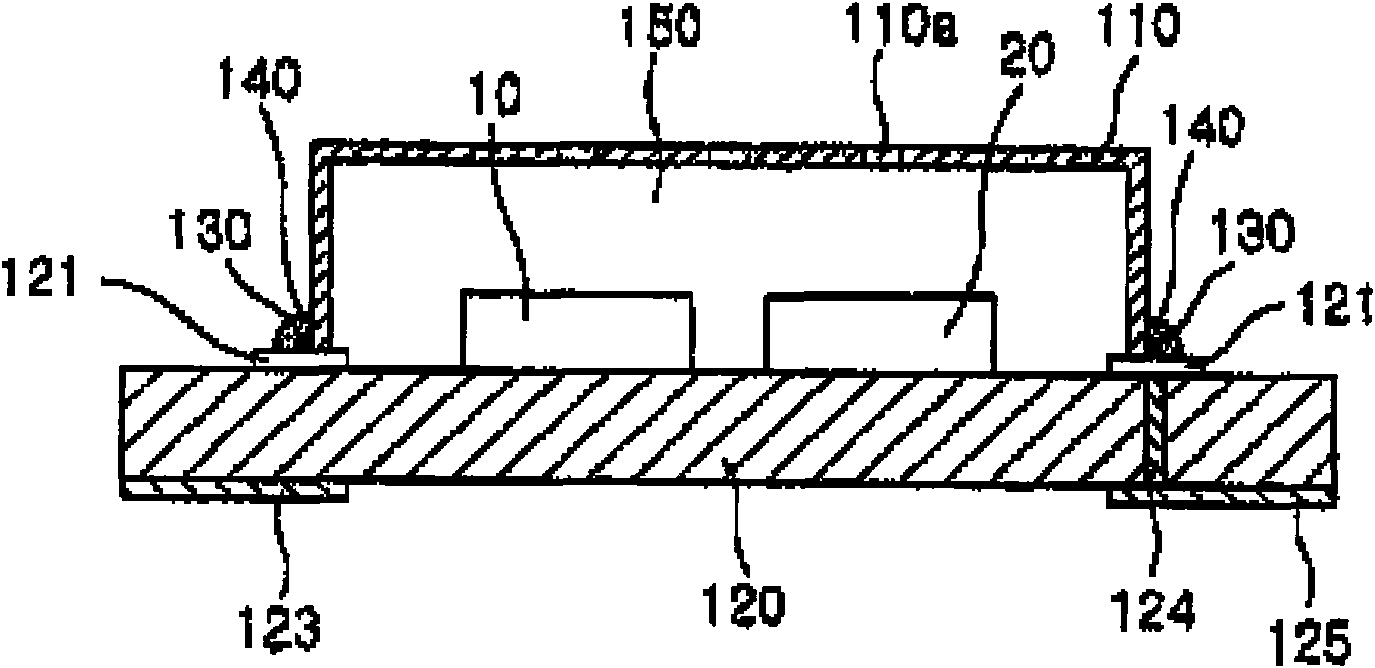
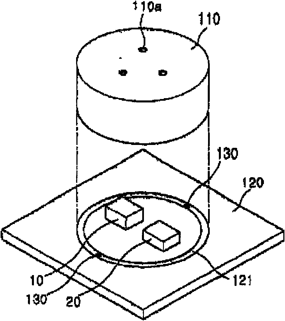
[0035] image 3 is a schematic diagram showing a specific structure of the MEMS microphone according to the first embodiment of the present invention. Such as image 3 As shown, the MEMS microphone that the present invention relates to comprises a square groove-shaped housing 1 and a square circuit board 3, and the open end 11 of the housing 1 and the square circuit board 3 are bonded together to form a square cavity of the MEMS microphone. A MEMS acoustic chip 2 for converting sound signals into electrical signals and an ASIC 4 for amplifying electrical signals are arranged in the cavity. The shell 1 is provided with a sound hole 5 for receiving external sound signals. And: the position on the circuit board 3 combined with the opening end 11 of the housing 1 is provided with a grounded annular conductive layer 31, the surface of the opening end 11 of the housing is set as an annular conductive surface, between the circuit board 3 and the opening end 11 of the housing 1 An ...

no. 2 example

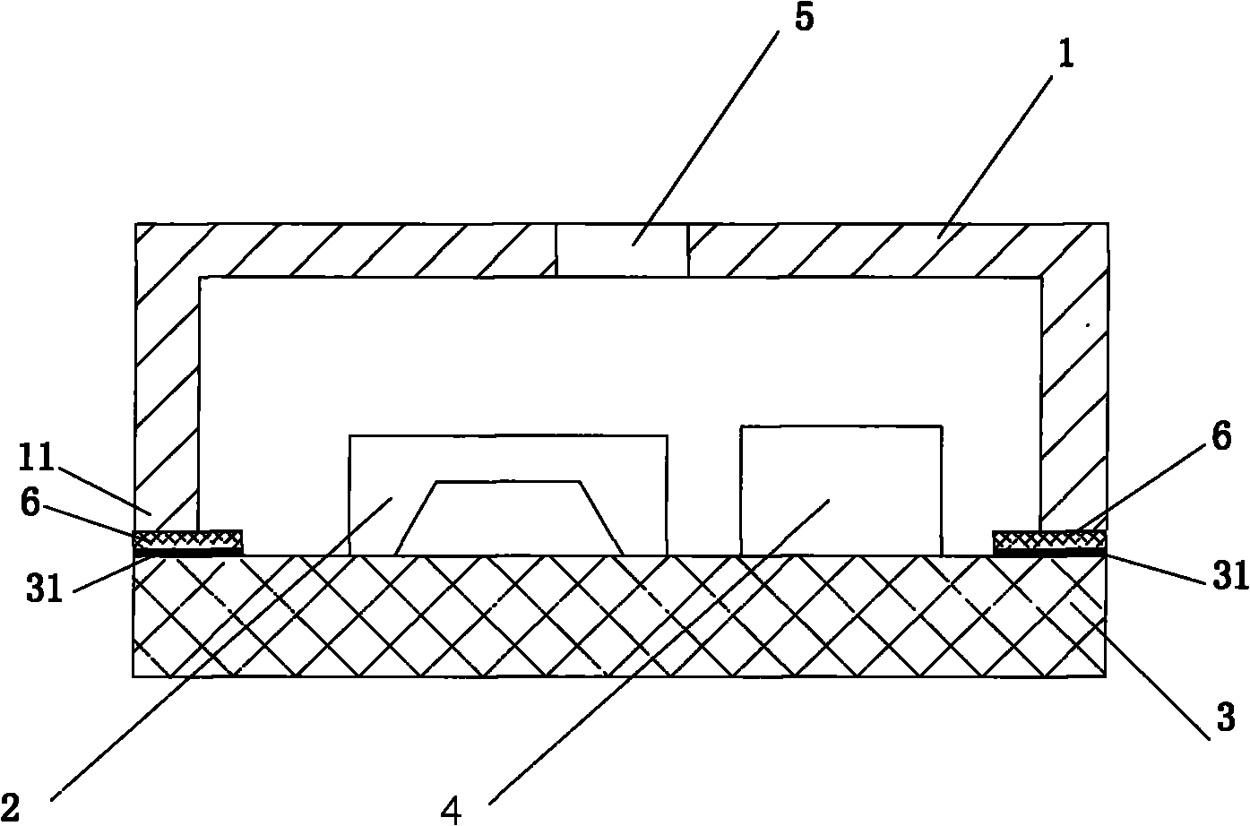
[0044] Figure 5 is a schematic diagram showing a specific structure of the MEMS microphone according to the second embodiment of the present invention. Such as Figure 5 As shown, the MEMS microphone includes a slot-shaped housing 1 and a circuit board 3, the open end 11 of the housing 1 and the circuit board 3 are bonded together to form the cavity of the MEMS microphone, and a sound signal conversion function is provided in the cavity. A MEMS acoustic chip 2 for electrical signals and an ASIC 4 for amplifying electrical signals. The shell 1 is provided with a sound hole 5 for receiving external sound signals. And: the position where the circuit board 3 is combined with the opening end 11 of the housing 1 is provided with a grounded annular conductive layer 31, the surface of the opening end 11 of the housing is set as an annular conductive surface, and the circuit board 3 and the opening end 11 of the housing 1 are arranged between There is an annular insulating adhesive g...


PUM

PropertyMeasurementUnit
Thicknessaaaaaaaaaa
Thicknessaaaaaaaaaa

Abstract

The invention provides a micro electro mechanical system (MEMS) microphone and an encapsulation method thereof. The MEMS microphone comprises a circuit board and a shell fixedly connected with the circuit board; the circuit board is combined with the opening end of the shell to form an encapsulation structure of the MEMS microphone; moreover, an annular insulation adhesive layer is arranged between the circuit board and the opening end of the shell; and the three parts, namely the surface of the opening end of the shell, the annular insulation adhesive layer, and the position, combined with the opening end of the shell, of the circuit board form a capacitor. In the MEMS microphone, the insulation adhesive layer instead of a conductive adhesive which has high boundedness, high cost and poor adhering effect is adopted between the shell and the circuit board; and by the technical scheme, the adhering process is simple, the production cost is reduced, and the large-scale popularization of the MEMS microphone is facilitated.

Description

technical field [0001] The invention relates to a microphone and a packaging method thereof, in particular to a MEMS microphone and a packaging method thereof. Background technique [0002] In recent years, MEMS microphones integrated with MEMS (micro-electromechanical systems) technology have begun to be applied in batches to electronic products such as mobile phones and notebooks. This kind of microphone has good high temperature resistance and can withstand the high temperature test of SMT technology. The general structure of this product is to use a circuit board and a shell to form a cavity to become the package of the MEMS microphone. On the outer surface of the circuit board, pads can be set to fix the MEMS microphone and electrically connect to the external circuit. The inside of the cavity is equipped with a MEMS acoustic chip, and the package of the microphone is provided with a sound hole that penetrates the inside and outside of the cavity and is used to receive ...

Claims


Application Information

Patent Timeline
IPC IPC(8): H04R19/04H04R31/00
Inventor 宋青林
Owner WEIFANG GOERTEK MICROELECTRONICS CO LTD
Why Eureka
Try Eureka