Display device, Cu alloy film for use in the display device, and Cu alloy sputtering target

A display device and alloy film technology, which is applied in the field of sputtering targets, can solve the problems of resin film deterioration and adhesion reduction, and achieve the effects of excellent adhesion, excellent etching characteristics, and reduced manufacturing costs

Inactive Publication Date: 2011-07-06
KOBE STEEL LTD
View PDF6 Cites 4 Cited by
  • Summary
  • Abstract
  • Description
  • Claims
  • Application Information

AI Technical Summary

Problems solved by technology

However, in this technique, the resin film deteriorates during high-temperature annealing during the manufacture of displays (such as liquid crystal panels), and the adhesiveness may decrease.

Method used


Image

  • Display device, Cu alloy film for use in the display device, and Cu alloy sputtering target
  • Display device, Cu alloy film for use in the display device, and Cu alloy sputtering target
  • Display device, Cu alloy film for use in the display device, and Cu alloy sputtering target

Examples


Embodiment 1

[0137] In order to evaluate the adhesion between the Cu alloy film and the glass substrate, a peeling test was performed using the following adhesive tape.

[0138] (production of samples)

[0139] First, on a glass substrate (manufactured by Corning Co., Ltd., Eagle 2000, diameter 100 mm x thickness 0.7 mm), pure Cu was formed with a film thickness of 300 nm at room temperature by DC magnetron sputtering (film formation conditions are as follows). film, pure Mo film or Cu alloy film with the composition shown in Table 1. Then, after film formation, heat treatment was carried out in a vacuum atmosphere at 350° C. for 30 minutes, and it was used as a sample for adhesiveness evaluation.

[0140] In addition, in forming the pure Cu film and the pure Mo film, pure Cu and pure Mo are used as sputtering targets, respectively. In addition, in the formation of Cu alloy films of various components, a pure Cu sputtering target provided with chips (chips) containing elements other than...

Embodiment 2

[0157] A Cu-X-containing alloy film was formed, and the influence of heat treatment after film formation on the adhesion to the glass substrate (the above-mentioned film residue rate) was investigated.

[0158] (production of samples)

[0159] On a glass substrate (manufactured by Corning Corporation, Eagle 2000, 100 mm in diameter x 0.7 mm in thickness), as in Example 1 above, various Cu-containing X alloys were formed with a film thickness of 300 nm by DC magnetron sputtering. Film (X=Al / Mg or Ti, X content is 0.1 at%, 2.0 at%, or 5.0 at%). Then, prepare the following samples respectively:

[0160] (A) The sample (as-deposited state sample) prepared as above;

[0161] (B) A sample subjected to heat treatment at 350° C. for 30 minutes in a vacuum atmosphere;

[0162] (C) A sample subjected to heat treatment at 400° C. for 30 minutes in a vacuum atmosphere;

[0163] (D) A sample subjected to heat treatment held at 450° C. for 30 minutes in a vacuum atmosphere.

[0164] (E...

Embodiment 3

[0168] A Cu-X-containing alloy film was formed, and the resistivity of the alloy film was measured and evaluated.

[0169] (production of samples)

[0170] On a glass substrate (manufactured by Corning Corporation, Eagle 2000, 100 mm in diameter x 0.7 mm in thickness), as in Example 1 above, various Cu-containing X alloys were formed with a film thickness of 300 nm by DC magnetron sputtering. Film (X=Al / Mg or Ti, X content is 0.1 at%, 2.0 at%, or 5.0 at%).

[0171] (measurement of resistivity)

[0172] The various Cu-X-containing alloy films formed above were subjected to photolithography and wet etching to form a stripe-like pattern (resistivity measurement pattern) with a width of 100 μm and a length of 10 mm, and then used the DC 4-probe method using a probe. , the resistivity of the pattern was measured at room temperature.

[0173] In addition, the measurement of electrical resistivity was also performed about each sample (striped pattern) of following (a)-(d).

[017...


PUM

PropertyMeasurementUnit
thicknessaaaaaaaaaa
electrical resistivityaaaaaaaaaa

Abstract

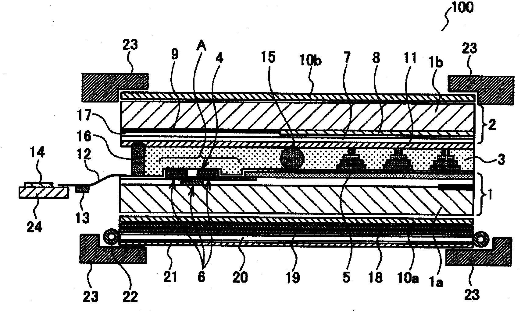
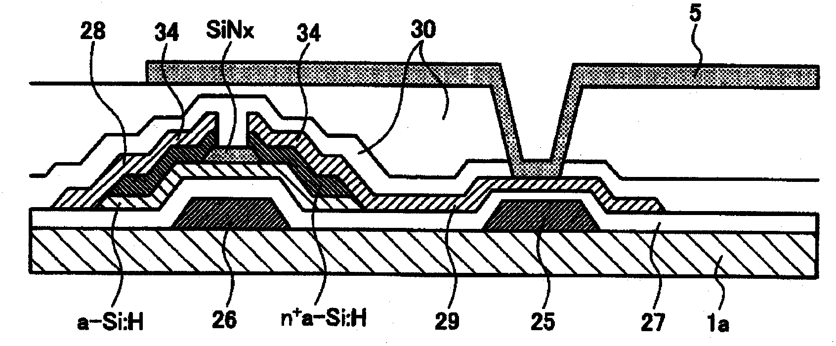
Disclosed is a Cu alloy film for a display device that has high adhesion to a glass substrate while maintaining low electric resistance characteristic of Cu-based materials. The Cu alloy film is wiring in direct contact with a glass substrate on a board and contains 0.1 to 10.0 atomic% in total of one or more elements selected from the group consisting of Ti, Al, and Mg. Also disclosed is a display device comprising a thin-film transistor that comprises the Cu alloy film. In a preferred embodiment of the display device, the thin-film transistor has a bottom gate-type structure, and a gate electrode and scanning lines in the thin-film transistor comprise the Cu alloy film and are in direct contact with the glass substrate.

Description

technical field [0001] The present invention relates to a display device and a Cu alloy film used therefor, and more particularly to a Cu alloy constituting wiring that is in direct contact with a glass substrate in a thin film transistor (Thin Film Transistor: hereinafter referred to as TFT) of a display device film, and the Cu alloy film are used for flat panel displays (display devices) such as liquid crystal displays and organic EL displays of the above-mentioned thin film transistors, and as sputtering targets for the formation of the above-mentioned Cu alloy film. In addition, in the following description, among the display devices, a liquid crystal display will be taken as an example, but it is not intended to be limited thereto. Background technique [0002] Liquid crystal displays are used in various fields ranging from small mobile phones to large televisions exceeding 100 inches, for example. The liquid crystal display is classified into a simple matrix type liqu...

Claims


Application Information

Patent Timeline
Patent Type & Authority Applications(China)
IPC IPC(8): C22C9/00C22C9/01G02F1/1343G09F9/30H01L21/3205H01L23/52H01L29/423H01L29/49H01L29/786
CPCH01L2924/0002C22C9/01H01L23/53233H01L27/1214C22C9/00H01L27/124Y10T428/265H01L2924/00C23C14/14C23C14/34
Inventor 大西隆三木绫后藤裕史水野雅夫伊藤弘高富久胜文
Owner KOBE STEEL LTD
Why Eureka
Try Eureka