Thyristor device

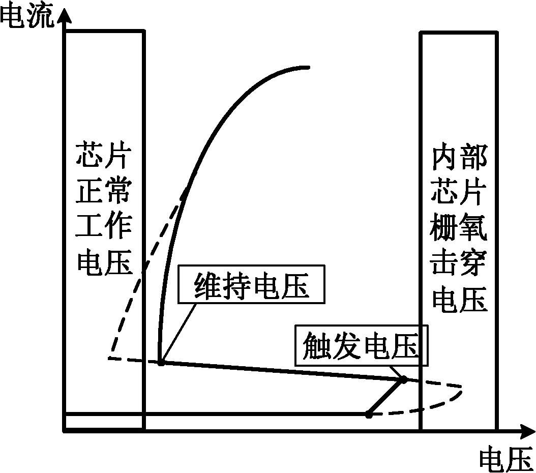
A technology of silicon device and injection area, applied in the direction of electric solid device, semiconductor device, electrical components, etc., can solve the problems of low thyristor maintaining voltage, affecting the normal operation of the chip, and the voltage cannot be effectively protected, and saving the layout area. , The effect of reducing the layout area and uniform current

Inactive Publication Date: 2011-08-03
ZHEJIANG UNIV
View PDF5 Cites 10 Cited by
  • Summary
  • Abstract
  • Description
  • Claims
  • Application Information

AI Technical Summary

Problems solved by technology

[0010] Therefore, in the prior art, the trigger voltage of the thyristor is generally high, which cannot effectively protect the working voltage of 5V and below; at the same time, the maintenance voltage of the thyristor is usually too low, which is prone to latch-up effect and affects the normal operation of the chip. Work

Method used


Image

  • Thyristor device
  • Thyristor device
  • Thyristor device

Examples


Embodiment Construction

[0027] The present invention will be described in detail below in conjunction with embodiments and drawings, but the present invention is not limited to this.

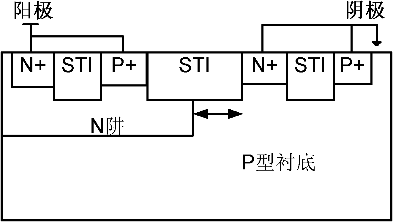
[0028] Such as Figure 4 with Figure 5 As shown, a thyristor device includes a P-type substrate 41. A first N-well 42 connected to an electrical anode and a second N-well 43 with a floating potential are arranged on the P-type substrate 41 along the lateral direction. The N well 42 and the second N well 43 are not connected;

[0029] From the first N well 42 to the direction of the second N well 43, in the first N well 42, the second N well 43 and the P-type substrate 41 in the region where no N well is provided, first N+ Injection zone 44, first P+ injection zone 45, third N+ injection zone 49, second N+ injection zone 46, and second P+ injection zone 47;

[0030] Wherein, the first N+ implantation region 44 and the first P+ implantation region 45 are arranged in the first N well 42, and the two ends of the third N+ impla...


PUM


Abstract

The invention discloses a thyristor device, which comprises a P-type substrate, wherein a first N well and a second N well are arranged on the P-type substrate; the first N well is connected with an anode; the potential of the second N well suspends; and a third N+ injection region is bridged between the two N wells and the P-type substrate. A triggering voltage value is reduced by bridging the third N+ injection region between the first N well and the P-type substrate, and a maintaining voltage value is increased by adding the second N well which has the suspending potential into the P-type substrate, so that the aim of a low-triggering and high-maintaining voltage is achieved. Moreover, the thyristor device is simple in structure, high in layout efficiency of unit area, uniform in current, good in robustness, and stable and reliable.

Description

Technical field [0001] The invention belongs to the field of electrostatic protection of integrated circuits, and specifically relates to a silicon controlled device. Background technique [0002] The phenomenon of electrostatic discharge (ESD) in nature poses a serious threat to the reliability of integrated circuits. In the industry, 30% of the failures of integrated circuit products are caused by electrostatic discharge, and the smaller and smaller process size and thinner gate oxide thickness greatly increase the probability of the integrated circuit being damaged by electrostatic discharge. Therefore, improving the reliability of integrated circuit electrostatic discharge protection has a non-negligible effect on improving the yield of products. [0003] There are generally four modes of electrostatic discharge phenomenon: HBM (human body discharge mode), MM (machine discharge mode), CDM (component charging and discharging mode), and electric field induction mode (FIM). The ...

Claims


Application Information

Patent Timeline
Patent Type & Authority Applications(China)
IPC IPC(8): H01L29/36H01L27/02H01L27/092
Inventor 苗萌董树荣李明亮吴健韩雁马飞宋波郑剑锋
Owner ZHEJIANG UNIV
Why Eureka
Try Eureka