Multi-layered circuit board and manufacturing method thereof

A technology of multilayer circuit boards and manufacturing methods, which is applied in the direction of multilayer circuit manufacturing, printed circuits, electrical components, etc., can solve problems such as circuit breakage, delaminated circuit boards, and large drop, so as to prevent delamination and improve conductivity. Through the quality, improve the effect of appearance quality

Active Publication Date: 2012-12-19
AVARY HLDG (SHENZHEN) CO LTD +1
View PDF0 Cites 0 Cited by
  • Summary
  • Abstract
  • Description
  • Claims
  • Application Information

AI Technical Summary

Problems solved by technology

However, during the thermocompression bonding process of the outer layer board and the inner layer board, the film will soften due to heat and become a molten state. When the thickness of the film is 25 μm, the drop at the edge of the opening area is 25 μm), so the gas trapped between the film and the outer or inner plate stays at the opposite edges of the opening area and cannot escape in time. Gas forms bubbles after thermocompression
In the subsequent processing of the multilayer circuit board, the bubbles will expand under heat to form a raised area, which not only affects the appearance quality of the multilayer circuit board, but also makes the multilayer circuit board easy to cause delamination during subsequent processing or use, causing the circuit board fail
Moreover, during the subsequent dry film lamination process of the multilayer circuit board, the copper layer of the outer layer board may be disconnected at the opening area of ​​the film due to the height difference, causing line breakage and affecting the conduction quality of the multilayer circuit board

Method used


Image

  • Multi-layered circuit board and manufacturing method thereof
  • Multi-layered circuit board and manufacturing method thereof
  • Multi-layered circuit board and manufacturing method thereof

Examples


Embodiment Construction

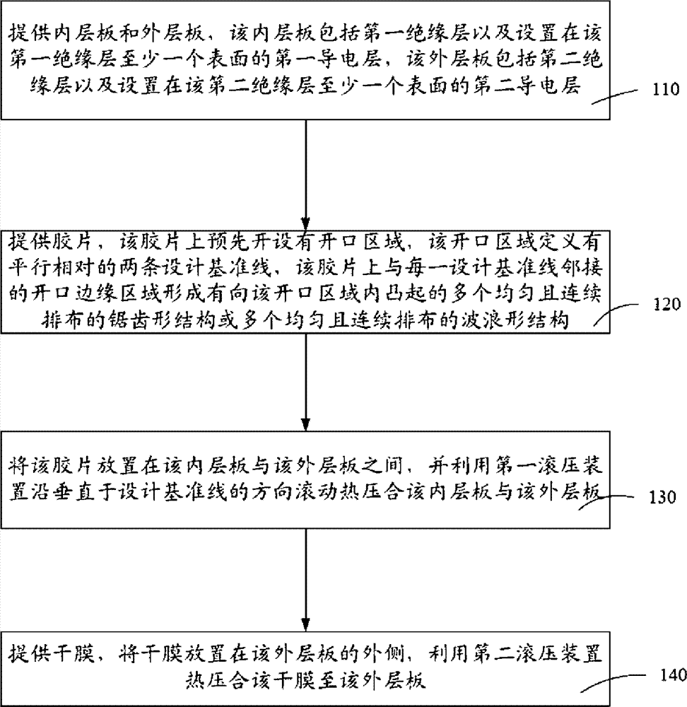
[0021] The multilayer circuit board of the present technical solution and its manufacturing method will be further described in detail below in conjunction with the drawings and embodiments.

[0022] see figure 1 , the embodiment of the technical solution provides a method for manufacturing a multilayer circuit board, which includes the following steps:

[0023] Step 110, providing an inner layer board and an outer layer board, the inner layer board includes a first insulating layer and a first conductive layer disposed on at least one surface of the first insulating layer, the outer layer board includes a second insulating layer and a first conductive layer disposed on at least one surface of the first insulating layer A second conductive layer on at least one surface of the second insulating layer.

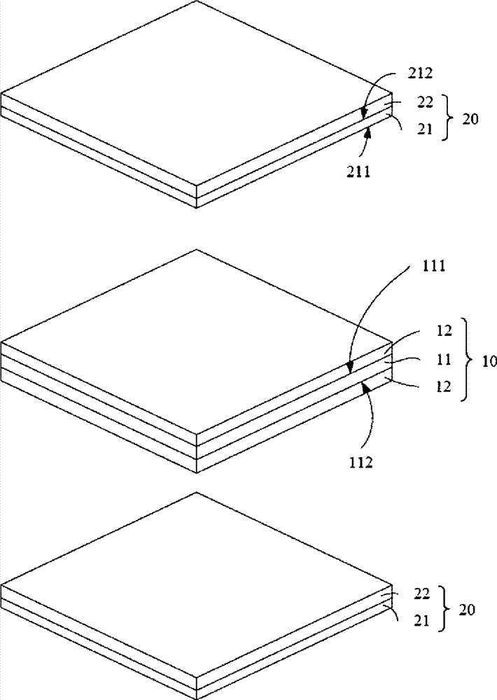
[0024] see figure 2 , the inner board 10 provided in this embodiment includes a first insulating layer 11 and a first conductive layer 12 . The first insulating layer 11 has...


PUM


Abstract

The invention provides a manufacturing method of a multi-layered circuit board, comprising the steps of: providing an inner-layer board and an outer-layer board; providing a film, presetting an opening area on the film, defining two parallel and opposite design reference lines for the opening area, forming a plurality of uniformly and continuously distributed sawtoothed structures or a plurality of uniformly and continuously distributed wavy structures which are convex towards the opening area at an opening edge area on the film adjacently connected with each design reference line; placing the film between the inner-layer board and the outer-layer board and utilizing a first rolling device to carry out thermocompression on the inner-layer board and the outer-layer board in a rolling manner along the direction vertical to the design reference lines; and providing a dry film, placing the dry film at the outer side of the outer-layer board, and utilizing a second rolling device to carry out thermocompression on the dry film to the outer-layer board. The invention also provides the multi-layered circuit board formed by utilizing the manufacturing method thereof.

Description

technical field [0001] The invention relates to circuit board technology, in particular to a multilayer circuit board with a specific adhesive layer structure and a manufacturing method thereof. Background technique [0002] With the rapid development of the electronic industry, the manufacturing technology of circuit boards, which are the basic components of electronic products, is becoming more and more important. The circuit board is generally made of a copper-clad substrate through a series of processes such as cutting, drilling, etching, exposure, development, pressing, and molding. For details, please refer to the article "Dielectric characterization of printed circuit board substrates" published by C.H.Steer et al. in Proceedings of the IEEE, Vol.39, No.2 (August 2002). [0003] Generally, a multilayer circuit board can be formed by thermocompression bonding of an inner layer board and an outer layer board. A film is arranged between the inner layer board and the ou...

Claims


Application Information

Patent Timeline
Patent Type & Authority Patents(China)
IPC IPC(8): H05K3/46H05K1/00
Inventor 郑建邦
Owner AVARY HLDG (SHENZHEN) CO LTD
Why Eureka
Try Eureka