Electronic tag

A technology of electronic tags and substrates, which is applied in the field of radio frequency identification, can solve problems such as poor adaptability of background materials, difficult realization of manufacturing process, and influence on application range, etc., and achieve the effect of maintaining radiation performance, reducing size, and expanding application range

Inactive Publication Date: 2011-08-10
SICHUAN ZHONGCE MICROGRID TECH CO LTD
View PDF4 Cites 11 Cited by
  • Summary
  • Abstract
  • Description
  • Claims
  • Application Information

AI Technical Summary

Problems solved by technology

Especially for passive RFID cards with small geometric dimensions, it is difficult to meet the requirements of antenna gain, resonance frequency and impedance matching with existing microstrip antennas and conventional design and manufacturing processes.
The technical difficulties in the design of electronic tag antennas working in the 910MHz frequency band (frequency range 860-960MHz) in the prior art are mainly: 1. The antenna size is large. The working frequency of this frequency band determines the electrical size of the electronic tag antenna in this frequency band. The current RF antenna design method will lead to large antenna size, which seriously affects its application range, so a new technology to reduce the antenna size must be adopted; 2. The adaptability to complex background materials is poor. It is sensitive to environments such as metals and liquids, which makes it difficult for passive tag antennas with this operating frequency to work in objects with metal surfaces or in liquid environments

Method used


Image

  • Electronic tag
  • Electronic tag
  • Electronic tag

Examples


Embodiment

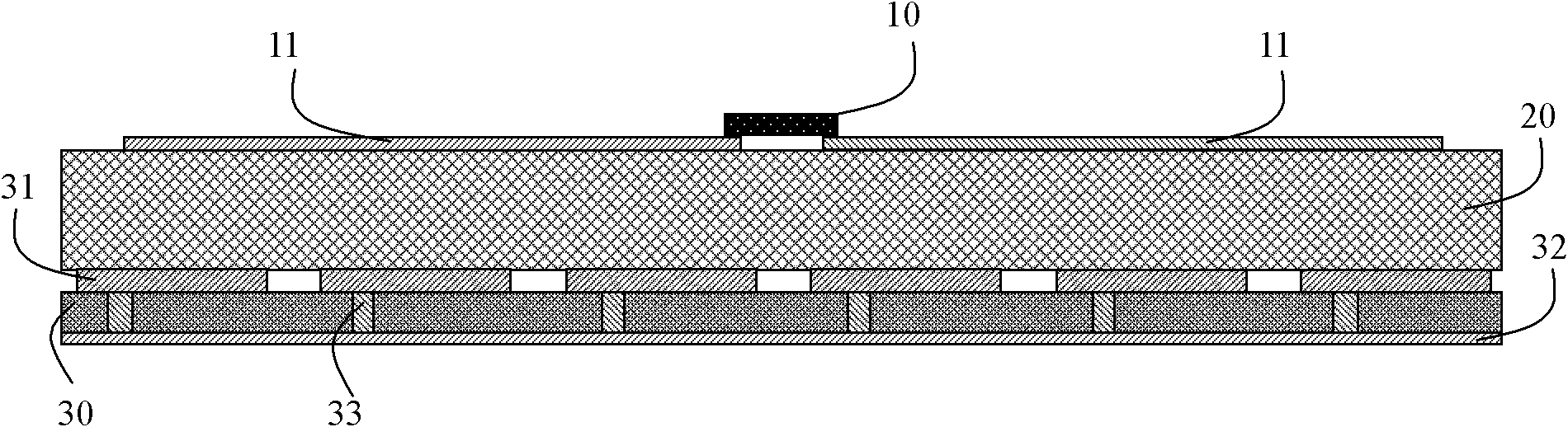
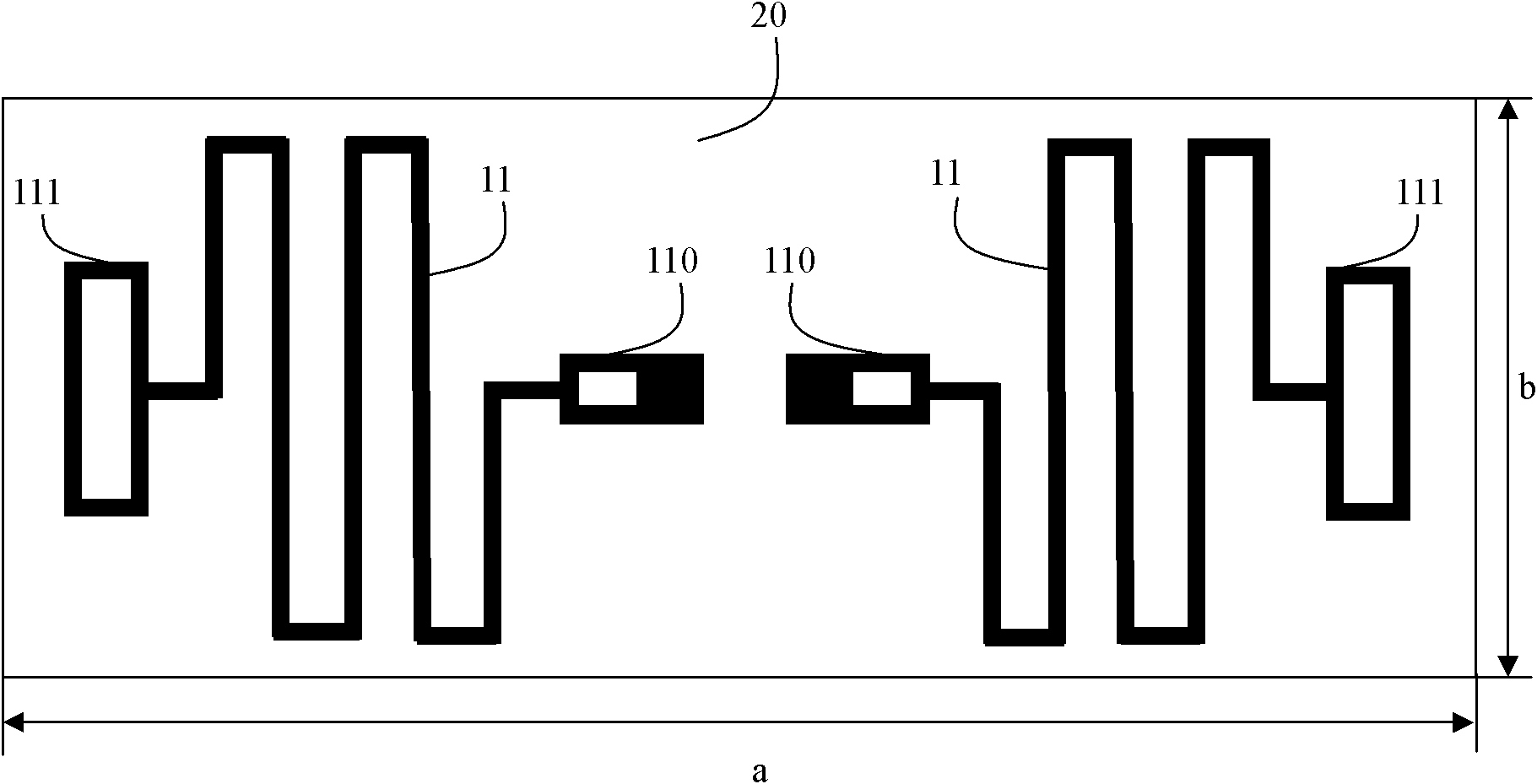
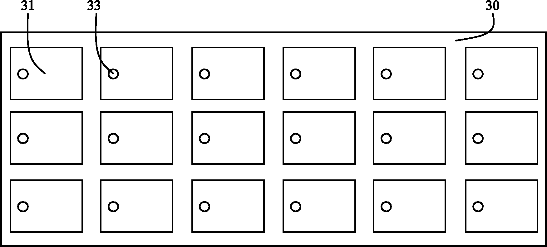
[0025] In this example, the electronic tag includes a substrate and a microstrip antenna. see figure 1 , figure 2 , image 3 and Figure 4 In this example, the substrate is composed of a support layer 20 , a metal patch layer 31 , a dielectric layer 30 and a metal ground 32 . Here, the metal patch layer 31 , the dielectric layer 30 and the metal ground 32 constitute the structure of the AMC. The specific manufacturing process is to form a metal film on the front and back of the dielectric layer. The material of the metal film used in this example is copper. The metal film on the front side of the dielectric layer 30 is etched to form metal sheets isolated from each other, forming the metal patch layer 31 ; an integral metal film on the back side of the dielectric layer forms the metal ground 32 . The metal patch layer can also be formed by pasting a rectangular metal sheet on the front of the dielectric layer 30 . In the AMC ground structure, each metal sheet on the fron...


PUM


Abstract

The invention relates to an electronic tag. The invention solves the technical problems of reducing the influence of a background material on an antenna and improving the environment adaptability of the electronic tag. The invention discloses the electronic tag, wherein the structure of the electronic tag comprises a substrate and a micro-strip antenna, and the micro-strip antenna is arranged on the substrate. The electronic tag is characterized in that: the substrate comprises a supporting layer, a metal patch layer, a medium layer and a metal ground; the micro-strip antenna is made on the front side of the substrate, the metal patch layer and the metal ground are attached to two sides of the medium layer respectively, the metal patch layer is contacted with the supporting layer, and the metal ground is positioned on the back of the substrate; and the metal patch layer consists of metal sheets mutually isolated on the front side of the medium layer, the metal ground consists of metal plates on the back of the medium layer, and each metal sheet is connected with the metal plate through a conductor passing through the medium layer. The electronic tag effectively weakens the influence of the complex background material such as metal, liquid and the like on the resonance frequency of the antenna, and can be used as a passive electronic tag of an ultra high frequency (UHF) band.

Description

technical field [0001] The invention relates to radio frequency identification technology, in particular to an electronic label. Background technique [0002] Radio Frequency Identification (RFID) technology is a non-contact automatic identification technology. Radio frequency identification technology uses radio frequency signals to achieve non-contact information transmission through spatial coupling, and achieves the purpose of identification through the transmitted information. Specifically, radio frequency identification is mainly through the mutual information transmission between the card reader (or called reader) and the electronic tag (or called radio frequency identification card) attached to the object to be identified, and the electronic tag is read by the card reader. information carried on it. Radio frequency identification technology has many outstanding advantages: non-contact operation, long-distance identification (up to several centimeters to tens of met...

Claims


Application Information

Patent Timeline
Patent Type & Authority Applications(China)
IPC IPC(8): G06K19/077
Inventor 邓建华王建
Owner SICHUAN ZHONGCE MICROGRID TECH CO LTD
Why Eureka
Try Eureka