Double-pulse test method for IGBT module

A test method, double-pulse technology, applied in the field of double-pulse test, can solve the problems of lack of guidance and reference for commercial application, failure to obtain dynamic characteristic parameters, lack of better test methods, etc., to achieve simple test circuit, low test risk, Reliable effect of the test method

A test method, double-pulse technology, applied in the field of double-pulse test, can solve the problems of lack of guidance and reference for commercial application, failure to obtain dynamic characteristic parameters, lack of better test methods, etc., to achieve simple test circuit, low test risk, Reliable effect of the test method

CN102156253AActive Publication Date: 2011-08-17CHINA EPRI SCIENCE & TECHNOLOGY CO LTD +2

Image

  • Double-pulse test method for IGBT module
  • Double-pulse test method for IGBT module
  • Double-pulse test method for IGBT module

Examples


Embodiment Construction

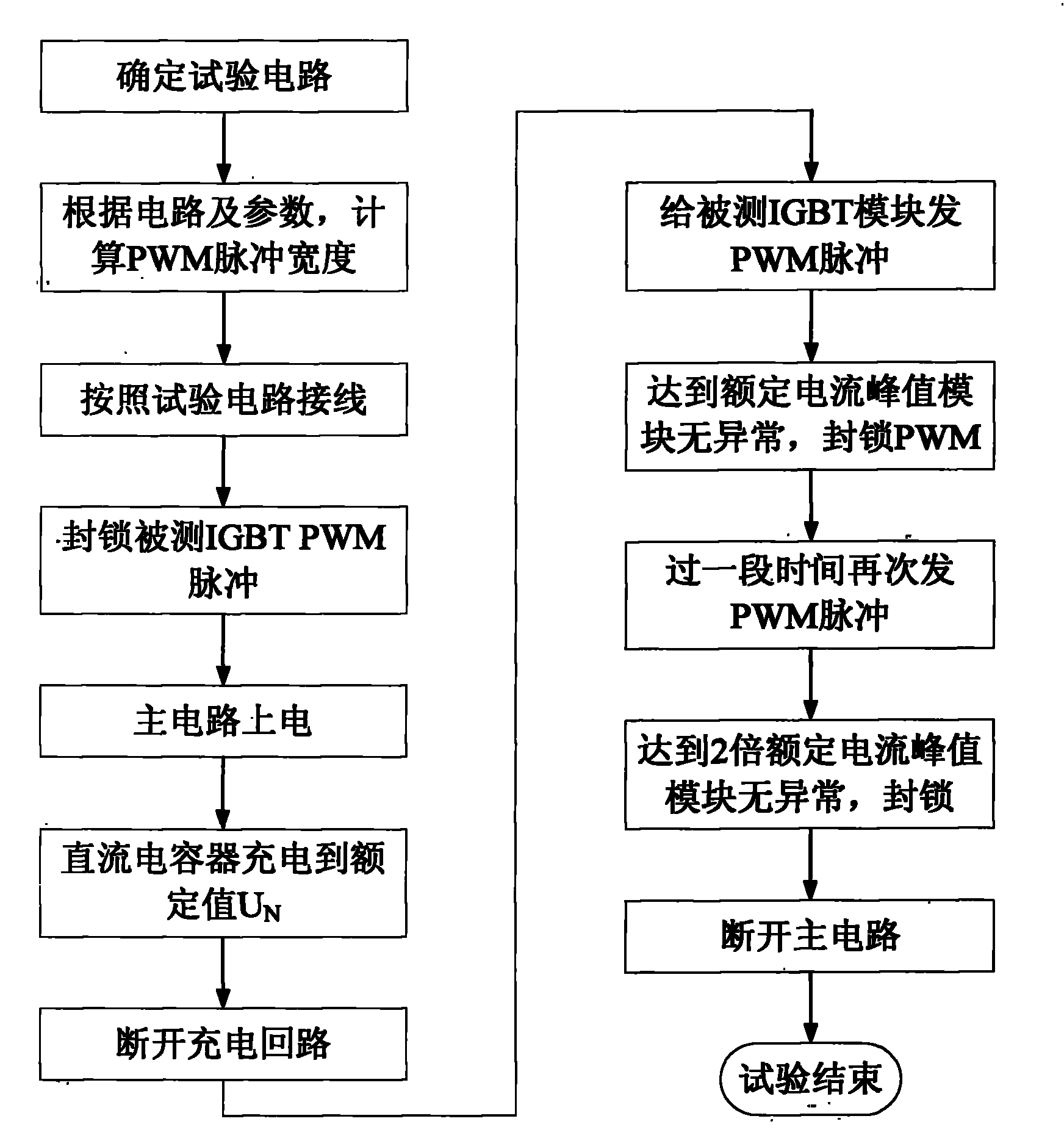
[0051] Method of the present invention specifically comprises the following steps:

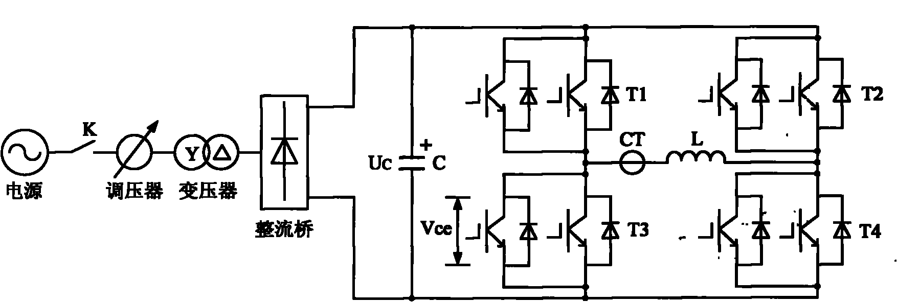
[0052] 1) Carry out test circuit wiring according to the test circuit diagram;

[0053] 2) After checking that the wiring is correct, the main circuit is switched on and powered on;

[0054] 3) The T1 and T4 tubes are always in the blocked state, and the T2 tube is in the open state, blocking the PWM pulse of the tested IGBT (T3 tube);

[0055] 4) Assuming that the capacitor is large, charge the DC capacitor to the rated value U N , the capacitor voltage remains basically unchanged after charging is completed;

[0056] 5) Disconnect the rectifier charging circuit;

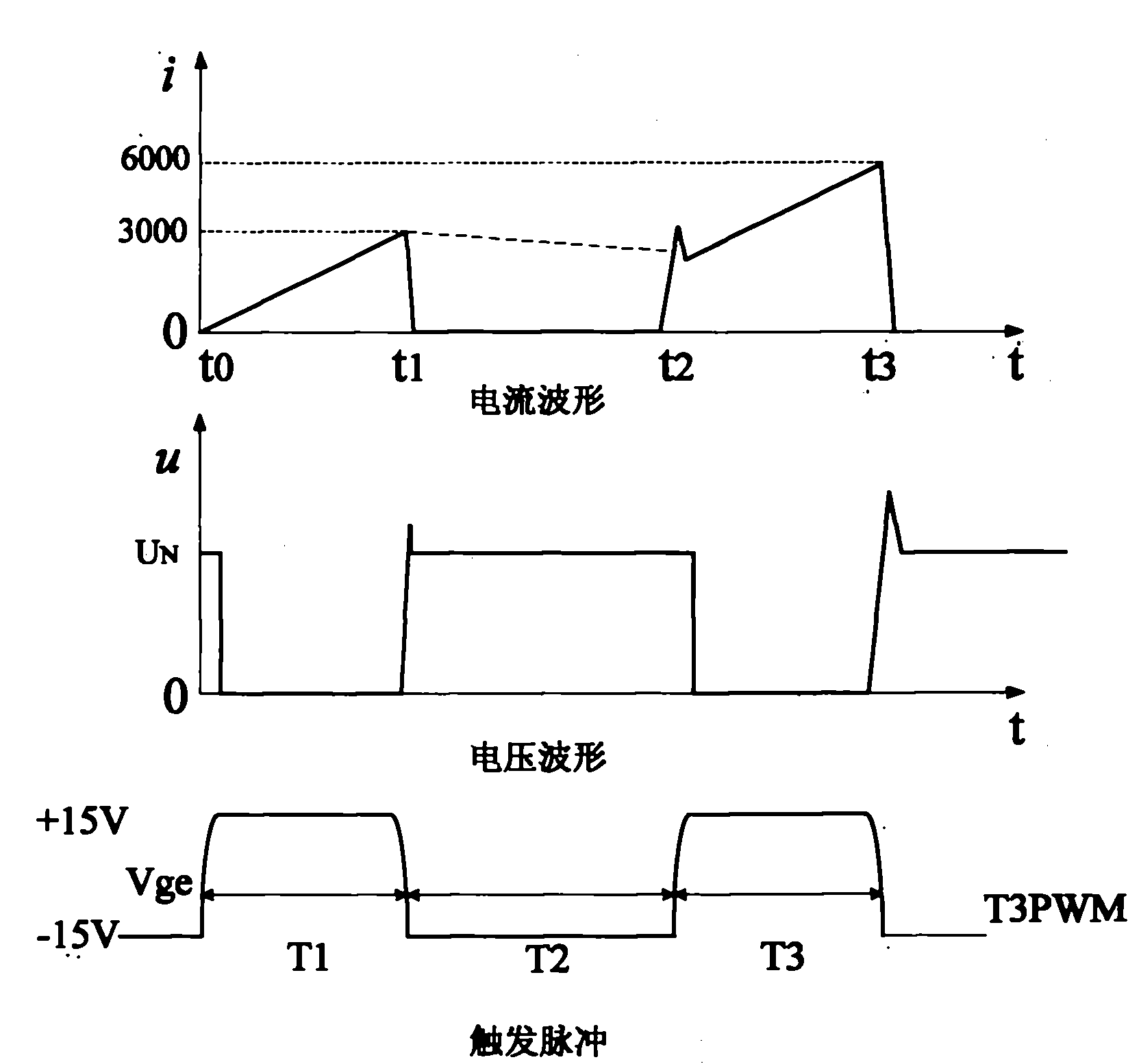
[0057] 6) Send a PWM pulse to the tested IGBT module (T3 tube), and T3 is turned on, so the DC capacitor C, the reactor L and the upper right IGBT T2 form a loop, and the current on the reactor increases linearly until it reaches the peak value of the rated current of the device I M , observe its conduction waveform through an...


PUM


Abstract

The invention belongs to the technical field of power semiconductor devices, and particularly relates to a double-pulse test method for an insulated gate bipolar transistor (IGBT) module. On and off of the tested IGBT module can be controlled by adding a driving positive voltage and a negative voltage between the grid and the emitter of the tested IGBT module; and two times of pulse width modulation (PWM) pulse are send to and blocked for the IGBT module, so that the IGBT module is subjected to an on-off-on-off process, the over current bearing capacity of the module and the capacity of mastering the on and off properties of the module are checked, and reference and basis are provided for application of the high-voltage and high-current IGBT module.

Description

technical field [0001] The invention belongs to the technical field of power semiconductor devices, and in particular relates to a double-pulse test method for an IGBT module. Background technique [0002] Insulated gate bipolar transistor IGBT belongs to the technical field of power semiconductor devices. Power semiconductor devices are high-power semiconductor devices used for power conversion and power control. Its development has gone through stages such as diodes, thyristors, and power transistors. [0003] Diode, also known as crystal diode, or diode for short, is an electronic component that only transmits current in one direction. It is a device with 2 terminals joined by 1 part number, and has the property of causing current to flow or not to flow according to the direction of the applied voltage. A crystal diode is a p-n junction formed by a p-type semiconductor and an n-type semiconductor, and a space charge layer is formed on both sides of the interface, and a s...

Claims


Application Information

Patent Timeline
17 Aug 2011
Publication
CN102156253A
IPC
G01R31/26; G01R31/327
Inventors
王轩; 王柯