
Plasma processing apparatus and plasma processing method

A plasma and processing device technology, applied in the field of plasma processing, can solve problems such as insufficient plasma density uniformity

Active Publication Date: 2015-05-06
TOKYO ELECTRON LTD
View PDF6 Cites 1 Cited by
  • Summary
  • Abstract
  • Description
  • Claims
  • Application Information

AI Technical Summary

Problems solved by technology

However, the uniformity of the plasma density obtained on the substrate is not sufficient in general plasma processes using only the usual RF antenna

Method used


Image

  • Plasma processing apparatus and plasma processing method
  • Plasma processing apparatus and plasma processing method
  • Plasma processing apparatus and plasma processing method

Examples


no. 1 approach

[0077] exist Figure 1 to Figure 10 The first embodiment of the present invention is described in .

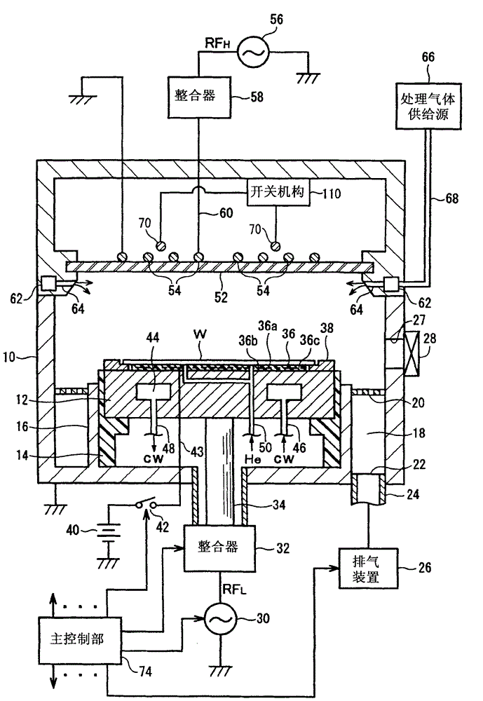
[0078] figure 1 The configuration of the inductively coupled plasma processing apparatus according to the first embodiment of the present invention is shown. This inductively coupled plasma processing apparatus is configured as a plasma etching apparatus using a planar coil-shaped RF antenna, and includes a cylindrical vacuum chamber (processing container) 10 made of metal such as aluminum or stainless steel. Chamber 10 is securely grounded.

[0079] First, the structure of each part not related to plasma generation in this inductively coupled plasma etching apparatus will be described.

[0080] In the lower center of the chamber 10, a disc-shaped susceptor 12 on which a substrate to be processed, for example, a semiconductor wafer W is placed, is horizontally arranged as a substrate holding table also serving as a high-frequency electrode. The base 12 is made of aluminum,...

no. 2 approach

[0130] Next, refer to Figure 11-1 4. Describe the second embodiment of the present invention.

[0131] exist Figure 11 The middle shows the configuration of the inductively coupled plasma processing apparatus in the second embodiment. In the figure, there is a device similar to the above-mentioned first embodiment ( figure 1 ) parts of the same structure or function are given the same symbols.

[0132] The second embodiment is characterized by including a variable resistance mechanism 120 instead of the switch mechanism 110 as compared to the first embodiment described above.

[0133] More specifically, the correction coil 70 is composed of an annular single-turn coil or a multi-turn coil that is open with a moderate gap g at both ends, and is coaxially arranged with respect to the RF antenna 54 so that the coil conductor is positioned at the RF antenna 54 in the radial direction. Between the inner circumference and the outer circumference of the coil 54 (preferably in t...

no. 3 approach

[0157] As another embodiment, it can also be configured such that the switch mechanism 110 in the above-mentioned first embodiment is replaced by Figure 18 The switch mechanism 150 is shown. The switch mechanism 150 has a switch 152 connected to both open ends of the correction coil 70 via a conductor, and a switch control circuit 154 that switches the ON / OFF state of the switch 152 based on an instruction from the main control unit 74 .

[0158] In this switch mechanism 150 , when the switch 152 is switched to the OFF state, no induced current flows through the correction coil 70 , so it is equivalent to a case where there is no correction coil 70 . When the switch 152 is switched to the closed (ON) state, the correction coil 70 is equivalent to a coil with both ends closed, and when the RF antenna 54 flows high-frequency RF H When a current is applied, an induced current flows through the correction coil 70 .

[0159] Such as Figure 19 As shown, it is also possible to a...


PUM


Abstract

The present invention provides a plasma processing apparatus and a plasma processing method therefore, capable of freely and accurately controlling the plasma density distribution by using a simple correction coil. In the inductively coupled plasma processing apparatus, an inductively coupled plasma is generated in the doughnut shape below the dielectric window 52 around the RF antenna 54 and then diffused in the large processing space, so that the density of the plasma becomes uniform around the susceptor 12 (i.e., on the semiconductor wafer W), especially in radial direction. The RF antenna 54 performs an electromagnetic field correction on the generated RF magnetic field by the correction coil 70 and controls the duty ratio of the induced current flowing in the correction coil 70 by the switching mechanism 110 depending on predetermined process parameters.

Description

technical field [0001] The present invention relates to the technique of implementing plasma processing on the substrate to be processed, in particular to an inductively coupled plasma processing device and a plasma processing method. Background technique [0002] In the processing of etching, stacking, oxidation, sputtering, etc. in the manufacturing process of semiconductor equipment and FPD (Flat Panel Display), plasma is often used in the processing gas in order to perform a good reaction at a relatively low temperature . In the prior art, for this kind of plasma treatment, plasma generated by high-frequency discharge in the MHz region is often used. Plasma generated by high-frequency discharge is roughly classified into capacitively coupled plasma and inductively coupled plasma as a more specific (device) plasma generating method. [0003] Generally, in an inductively coupled plasma processing apparatus, a dielectric window constitutes at least a part (for example, th...

Claims


Application Information

Patent Timeline
Patent Type & Authority Patents(China)
IPC IPC(8): H01J37/32H01L21/00H05H1/46
CPCH01J37/321H01J37/3211H01J37/32174H05H1/46H05H1/4652
Inventor 山泽阳平舆水地盐齐藤昌司传宝一树山涌纯
Owner TOKYO ELECTRON LTD
Learn More