Manufacturing method of protection circuit for array unit of image sensor

A technology of image sensor and array unit, which is applied in the direction of circuit, semiconductor/solid-state device manufacturing, electrical components, etc., can solve the problem of no static protection and achieve the effect of easy cutting

Active Publication Date: 2011-08-17
CARERAY DIGITAL MEDICAL TECH CO LTD
View PDF3 Cites 10 Cited by
  • Summary
  • Abstract
  • Description
  • Claims
  • Application Information

AI Technical Summary

Problems solved by technology

In the manufacturing process of the image sensor, it generally needs to go through more than 10 layers of photomasks to complete the process. After forming the TFT, it needs to go through additional layers

Method used


Image

  • Manufacturing method of protection circuit for array unit of image sensor
  • Manufacturing method of protection circuit for array unit of image sensor
  • Manufacturing method of protection circuit for array unit of image sensor

Examples


Embodiment Construction

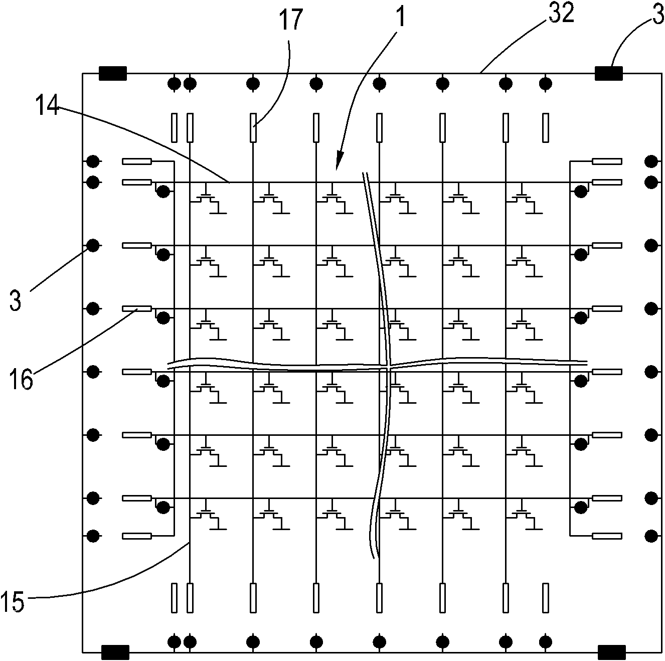
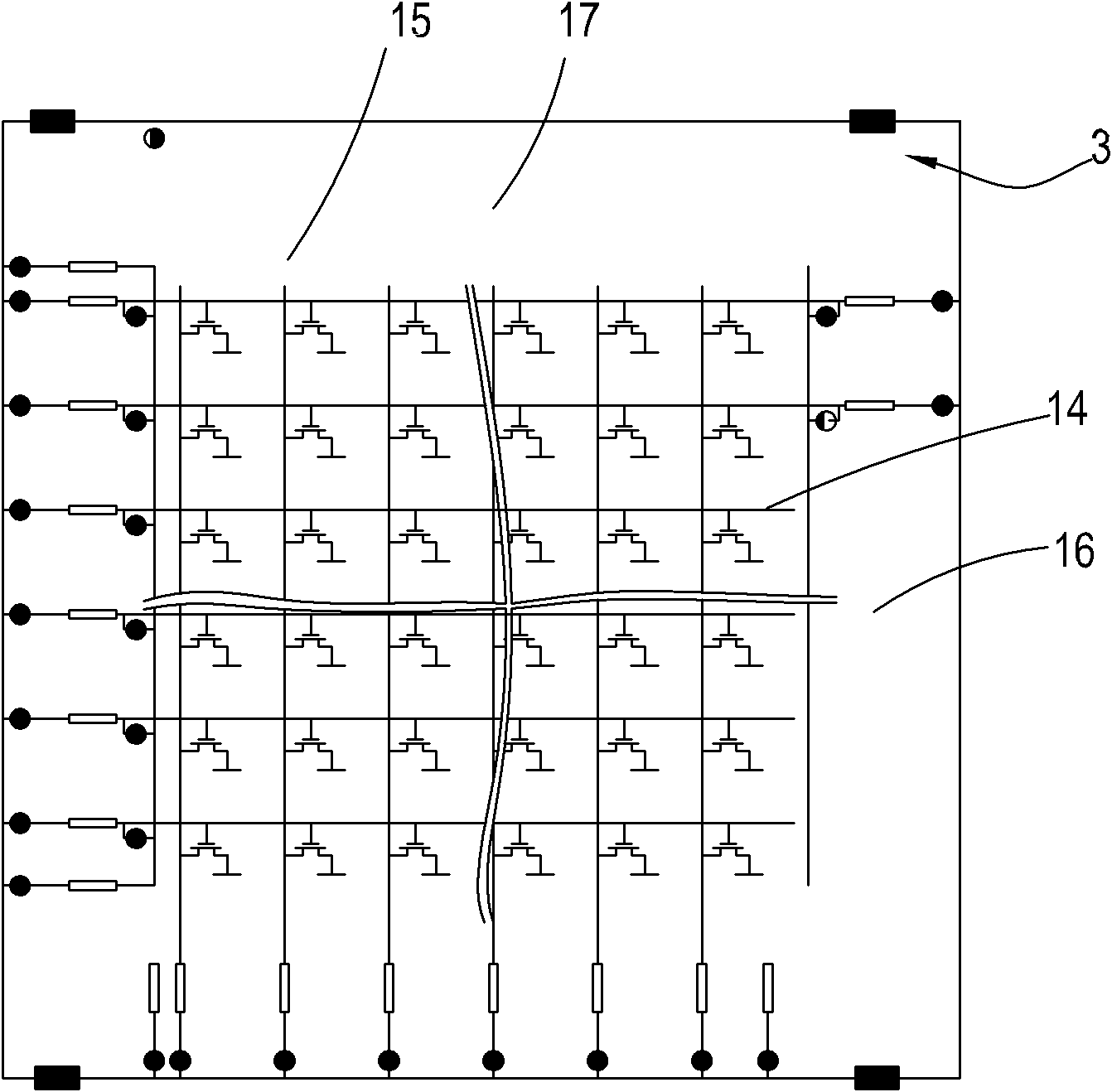
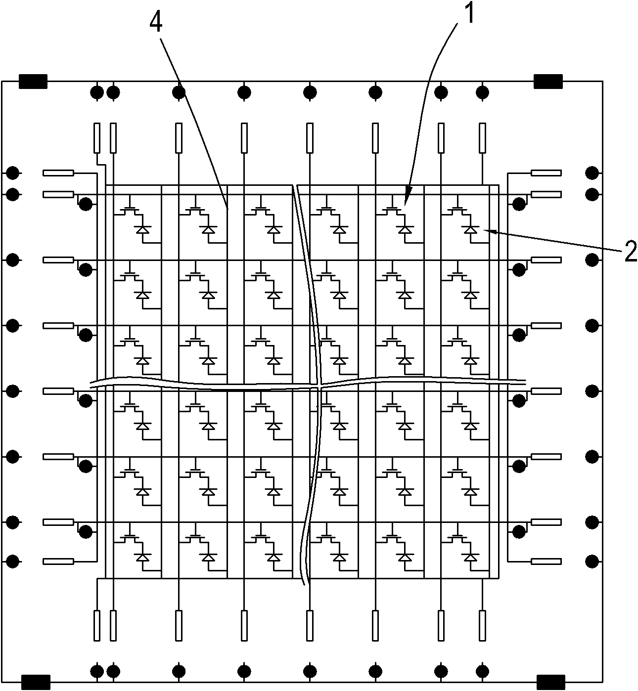
[0052] The present invention will be further described below in conjunction with the accompanying drawings and embodiments. The positional relationship of "up" and "down" described in this Figure 8 Corresponds to the upper and lower positional relationships shown in .

[0053] See attached Figure 8-17 , a method for manufacturing a protection circuit for an array unit of an image sensor, comprising the steps of:

[0054] A glass substrate 10 is provided, and the glass substrate 10 has at least one active region and a non-active region arranged on the periphery of the active region;

[0055] A. TFT generation process:

[0056] A1), see attached Figure 8 As shown, the first conductive layer M1 is deposited on the glass substrate 10, the gate electrode 11 of the pixel TFT1 is formed in the active area by etching process, and the gate electrode 11 of the pixel TFT1 is formed in the non-active area. The gate electrode 11 of the pixel TFT1 is connected to the scanning termina...


PUM


Abstract

The invention relates to a manufacturing method of a protection circuit for an array unit of an image sensor, which comprises the following steps: A) the process step of generating a TFT (thin-film transistor): manufacturing the pixel TFT in an active region of a glass substrate, forming an outer protection loop circuit in a non-active region of the glass substrate, and forming a signal line, a scanning line, a signal end pin electrode and a scanning end pin electrode on the glass substrate; B) the metal connection process step: using a metal material to connect the scanning end pin electrode and the signal end pin electrode with the outer protection loop circuit for forming an electrostatic discharge loop; C) the process step of generating a photosensitive diode: forming the photosensitive diode above the metal material; D) the etching process step: selectively etching the metal material between the scanning end pin electrode, the signal end pin electrode and the outer protection loop circuit; and E) the re-connection process step: using a transparent conductive material to re-connect the signal end pin electrode and the scanning end pin electrode with the outer protection loop circuit for forming the electrostatic discharge loop.

Description

technical field [0001] The invention relates to a method for manufacturing a protective circuit of an array unit of an amorphous silicon image sensor. Background technique [0002] Display devices and image sensors are the two main application areas for active matrix substrates. The active matrix substrate is divided into an active area (active area, Active area) and a non-active area. TFTs, scanning lines and signal lines, as well as storage capacitors or photodiodes are formed in the active area. The area is formed with pins for connecting the scanning lines and the driving circuit and pins for connecting the reading circuit and the signal lines. In order to prevent electrostatic damage, an electrostatic protection circuit is usually provided in the non-active area, and the pins of the scanning end and the pins of the signal end are respectively connected to the electrostatic protection circuit through conductive materials, such as the Chinese patent with the announcement...

Claims


Application Information

Patent Timeline
IPC IPC(8): H01L21/77H01L27/02H01L27/146
Inventor 王恒和刘建强
Owner CARERAY DIGITAL MEDICAL TECH CO LTD
Why Eureka
Try Eureka