Manufacturing method of organic electroluminescence element and image display system

A technology of electroluminescence components and image display systems, which is applied in the fields of electrical components, semiconductor/solid-state device manufacturing, and electric solid-state devices, and can solve the problems of large electrical differences in thin-film transistors, etc., to increase complexity and improve electrical differences If it is too large, the effect of increasing the aperture ratio

Active Publication Date: 2011-08-17
INNOLUX CORP
View PDF1 Cites 0 Cited by
  • Summary
  • Abstract
  • Description
  • Claims
  • Application Information

AI Technical Summary

Problems solved by technology

[0006] In view of the above problems, several preferred embodiments of the present invention improve the problem of excessive electrical differences between thin film transistors by adding a protection film.

Method used


Image

  • Manufacturing method of organic electroluminescence element and image display system
  • Manufacturing method of organic electroluminescence element and image display system
  • Manufacturing method of organic electroluminescence element and image display system

Examples


no. 1 Embodiment

[0023] Figure 2a-2f It is a cross-sectional view illustrating a manufacturing method of an organic electroluminescent element in a preferred embodiment of the present invention.

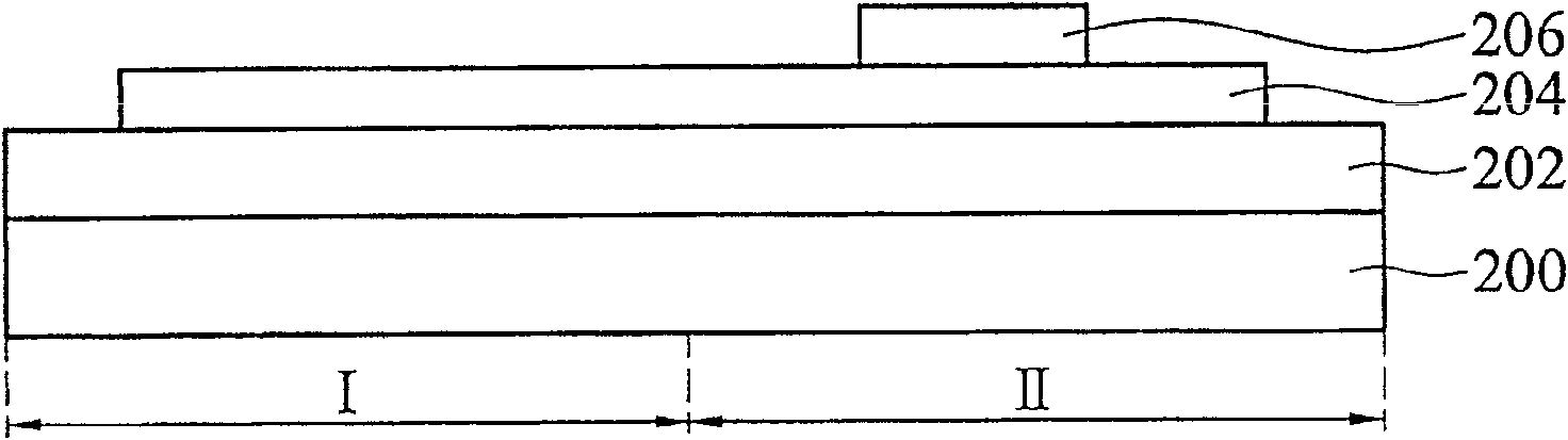
[0024] Such as Figure 2a As shown, sequentially on the substrate 200 including the first element region (eg, switching thin film transistor (switching thin film transistor) region I) and the second element region (eg, driving thin film transistor (driving thin film transistor) region II) A buffer layer 202 , an amorphous silicon layer 204 and a protection film 206 are formed. Wherein, the protection film 206 is formed on the portion of the amorphous silicon layer 204 in the second device region II; and the protection film 206 includes a material based on silicon, such as silicon oxide (SiOx), silicon nitride (SiNx) , silicon oxynitride (SiOxNy), or a stacked structure of silicon oxide and silicon nitride.

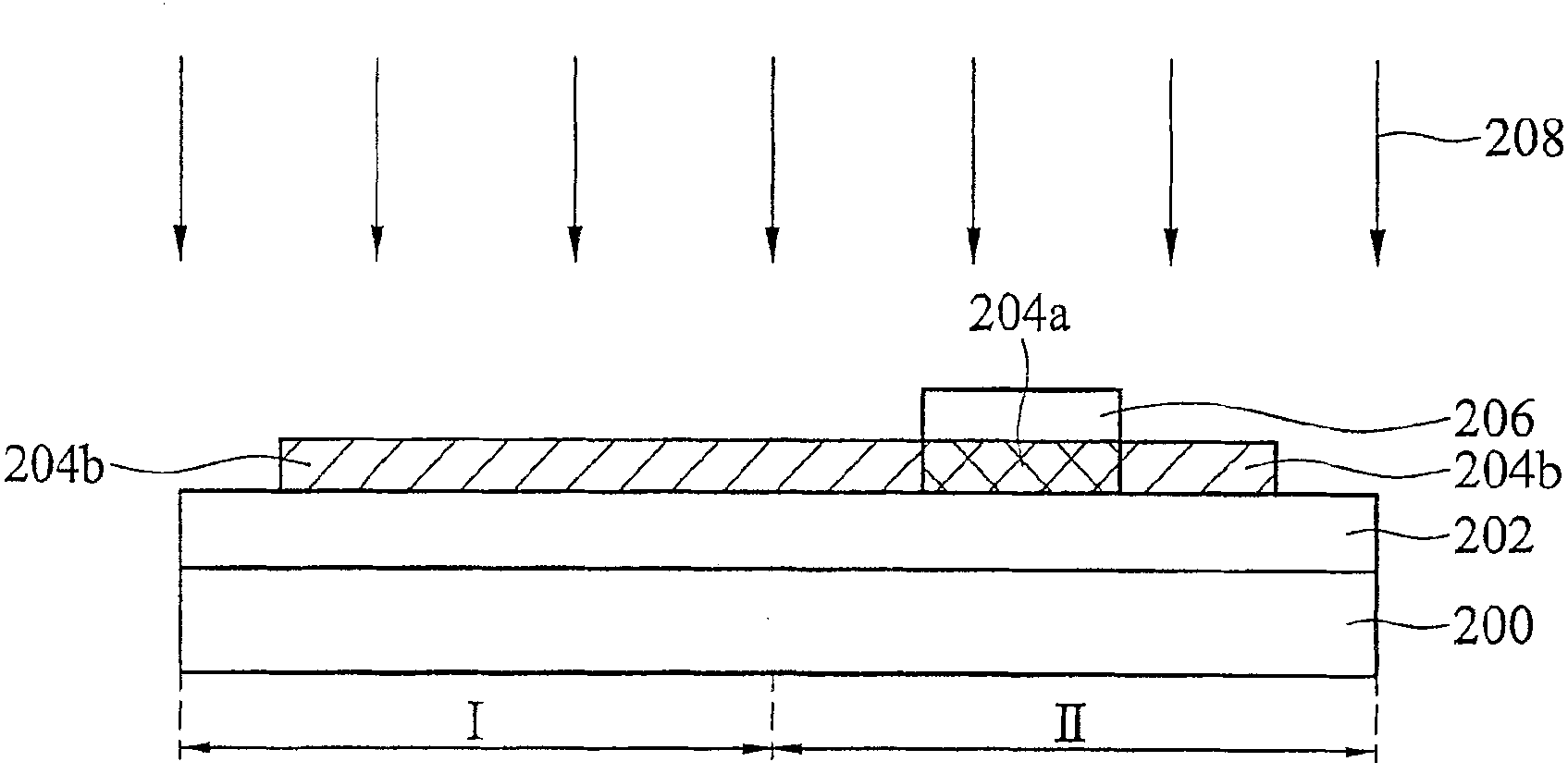
[0025] Such as Figure 2b As shown, an excimer laser annealing process 208 is performed ...

no. 2 Embodiment

[0030] Figure 3a ~ 3f It is a cross-sectional view illustrating a manufacturing method of an organic electroluminescent element in another preferred embodiment of the present invention.

[0031] Such as Figure 3a As shown, a buffer layer 302 and an amorphous silicon layer 304 are sequentially formed on a substrate 300 including a switching thin film transistor region I and a driving thin film transistor region II.

[0032] Such as Figure 3b As shown, the amorphous silicon layer 304 is patterned to form a patterned amorphous silicon layer 304b located in the switching thin film transistor region I and a patterned amorphous silicon layer 304a located in the driving thin film transistor region II.

[0033] Such as Figure 3c As shown, a protective film 306 covering the surface of the patterned amorphous silicon layer 304 a and part of the buffer layer 302 is formed. The protective film 306 includes a silicon-based material, such as silicon oxide (SiOx), silicon nitride (Si...

no. 3 Embodiment

[0038] Figure 4a~4g It is a cross-sectional view illustrating a manufacturing method of an organic electroluminescence device in another preferred embodiment of the present invention.

[0039] Such as Figure 4a As shown, a patterned protection film 402 is formed on a substrate 400 including a switching thin film transistor region I and a driving thin film transistor region II. The above-mentioned patterned protective film is located in the region II of the driving thin film transistor. The material of the patterned protection film 402 includes silicon oxide (SiOx), silicon nitride (SiNx), silicon oxynitride (SiOxNy), or a stacked structure thereof.

[0040] Such as Figure 4b As shown, a buffer layer 404 is formed on the patterned protection film 402 and the substrate 400 . Next, an amorphous silicon layer 406 is formed on the buffer layer 404, such as Figure 4c shown.

[0041] Such as Figure 4d As shown, an excimer laser annealing process 408 is performed on the am...


PUM


Abstract

The invention provides a manufacturing method of an organic electroluminescence element, which comprises the following steps: providing a substrate, wherein the substrate comprises a first element region and a second element region; forming an amorphous silicon layer above the substrate; forming a protective film at the part in the second element region, which is positioned above the amorphous silicon layer; performing a quasi-molecular laser annealing process on the amorphous silicon layer so as to convert the amorphous silicon layer into a polysilicon layer; removing the protective film; patterning the polysilicon layer so as to form a first patterned polysilicon layer in the first element region and form a second patterned polysilicon layer in the second element region, wherein the grain size of the first patterned polysilicon layer is larger than that of the second patterned polysilicon layer; and finally forming the organic electroluminescence element.

Description

[0001] This application is a divisional application of the invention patent application with the application number 200610137737.3 and the title of the invention "Manufacturing method of organic electroluminescence element and image display system". technical field [0002] The invention relates to a method for manufacturing an electroluminescence element, and in particular to a method for manufacturing a thin film transistor. Background technique [0003] Generally speaking, thin film transistors mainly include amorphous silicon thin film transistors and polysilicon thin film transistors. The array substrate of an existing electroluminescent device display (electroluminescent device display) can be divided into a light-emitting area and a circuit area, and the manufacturing method of the array substrate mainly includes: forming a thin film transistor (thin film transistor; TFT), forming a pixel electrode, and forming Organic Light Emitting Diodes. Wherein, the process of t...

Claims


Application Information

Patent Timeline
IPC IPC(8): H01L21/77H01L21/336H01L27/32G09F9/00
Inventor 詹川逸刘俊彦曾章和
Owner INNOLUX CORP
Why Eureka
Try Eureka