High-pixel photographic module and burning method for chip

The technology of a camera module and a burning method is applied in the direction of image communication, color TV parts, TV system parts, etc. It can solve the problems of small size of read-only memory, scrapping of modules, increase of cost, etc., and achieve good results. Technical advantages and technical effects, improvement of yield and production efficiency, and improvement of brightness uniformity

Active Publication Date: 2011-08-17
NINGBO SUNNY OPOTECH CO LTD
View PDF5 Cites 10 Cited by
  • Summary
  • Abstract
  • Description
  • Claims
  • Application Information

AI Technical Summary

Problems solved by technology

[0008] First, due to the addition of an electrically erasable programmable read-only memory, the production cost is actually increased, and at the same time, due to the addition of a step process, the production yield and production efficiency are reduced;
[0009] Secondly, because the above-mentioned EEPROM itself has a read / write pin to control it, since we need to keep the EEPROM in the writing state, so the During operation, there is a danger that the data in the EEPROM may be erased
[0010] In addition, since the EEPROM itself has a certain space, if the customer needs to adopt the socket solution, the EEPROM cannot be placed in it;
[0011] Moreover, due to the relatively small size of the EEPROM, it is very difficult to repair or replace, so some components of this module may be scrapped or the entire module may be scrapped directly
[0012] These shortcomings make the high-pixel camera module adopting the scheme of electrically erasable programmable read-only memory hinder its large-scale promotion and use to a certain extent.

Method used


Image

  • High-pixel photographic module and burning method for chip
  • High-pixel photographic module and burning method for chip
  • High-pixel photographic module and burning method for chip

Examples


Embodiment Construction

[0034] The present invention will be described in further detail below in conjunction with the accompanying drawings.

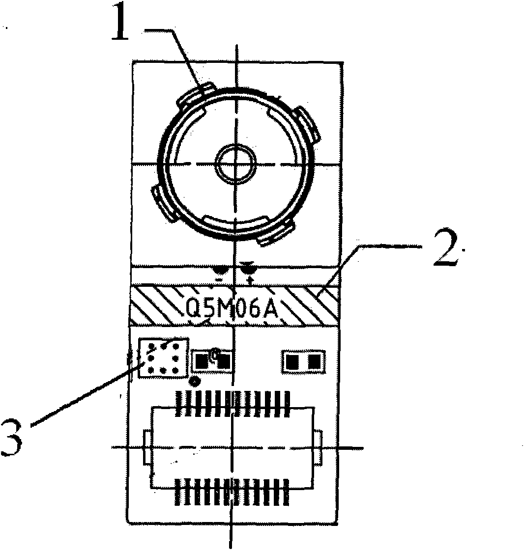
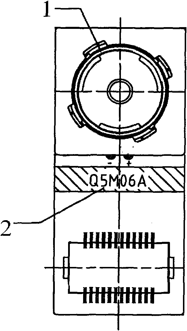
[0035] figure 2 It is a structural schematic diagram of a specific embodiment of the high-pixel camera module of the present invention.

[0036] As shown in the figure, compared with the existing design, this embodiment removes the electrically erasable programmable read-only memory (EEPROM), and adopts an integrated one-time programmable chip (OTP, not shown in the figure) The optical detection element 1 is fixed on the circuit board 4 by welding or other methods, and a black silver foil 2 is arranged below the optical detection element 1 .

[0037] Moreover, in the one-time programmable chip integrated with the above-mentioned optical detection element, the lens conformity compensation parameter (LSC) corresponding to the photosensitive optical detection element is burned, and the reading format of the above-mentioned parameter is set in the software of t...


PUM


Abstract

The invention discloses a high-pixel photographic module, which comprises an optical detection element, a programmable chip and a circuit board for fixing the optical detection element and the programmable chip. The high-pixel photographic module is characterized in that: the programmable chip is a one-time programmable chip; moreover, the photosensitive optical detection element is integrated with the chip; a camera consistence compensation parameter of the optical detection element is burnt in the chip; and mobile phone software reads the parameter by a preset format so as to correct the optical accuracy of the optical detection element. Compared with the conventional high-pixel photographic module structure, the invention reduces the size of the whole module, widens the application range of the module, simultaneously can increase the yield and improve the production efficiency in module batch production, shortens the time and achieves technical advantages and good technical effects. In addition, the invention also discloses a burning method for the chip of the high-pixel photographic module.

Description

technical field [0001] The solution belongs to the field of optoelectronics and relates to a high-pixel camera module. At the same time, the invention also relates to a method for burning a one-time programmable chip integrated on an optical detection element of the module. Background technique [0002] With the development of mobile phone technology, the application of camera modules has been greatly promoted. [0003] The structure of the current high-pixel camera module mainly includes a circuit board with an optical detection element (sensor) and an electrically erasable programmable read-only memory (EEPROM) provided with various parameters of the optical detection element. If the addressing mode of the above parameters is set internally, the optical detection element can be adjusted more accurately by software, so as to obtain a better camera effect. [0004] figure 1 It is a structural schematic diagram of a high-pixel camera module in the prior art. [0005] As sh...

Claims


Application Information

Patent Timeline
Patent Type & Authority Applications(China)
IPC IPC(8): H04M1/725G06F9/445H04N5/225H04M1/72406
Inventor 蔡赞赞徐永松徐重耀史慧波
Owner NINGBO SUNNY OPOTECH CO LTD
Why Eureka
Try Eureka