Semiconductor structure having an air-gap region and a method of manufacturing the same

An air-gap pattern, semiconductor technology, used in semiconductor/solid-state device manufacturing, semiconductor devices, semiconductor/solid-state device components, etc., can solve problems such as IC failure, electronic or structural integrity problems, demarcation cracks, etc., to achieve coverage The effect of increased rate and small effective dielectric constant

Active Publication Date: 2011-08-24
TAIWAN SEMICON MFG CO LTD
View PDF3 Cites 11 Cited by
  • Summary
  • Abstract
  • Description
  • Claims
  • Application Information

AI Technical Summary

Problems solved by technology

However, air gaps often cause problems with the electronic or structural integrity of the IC, for example, IC failure due to a newly formed via plug inadvertently hitting one of the multiple air gaps, or subsequent Delineation or cracking due to stress experienced during the bonding or encapsulation process

Method used


Image

  • Semiconductor structure having an air-gap region and a method of manufacturing the same
  • Semiconductor structure having an air-gap region and a method of manufacturing the same
  • Semiconductor structure having an air-gap region and a method of manufacturing the same

Examples


Embodiment Construction

[0067] The making and using of several illustrative embodiments are discussed in detail below. It should be appreciated, however, that the present disclosure provides many applicable concepts that can be embodied in a wide variety of specialized fields. The specific embodiments discussed are illustrative only, and do not limit the scope of the present disclosure. Alternative embodiments will also be appreciated by those skilled in the art.

[0068] As mentioned above, it is very important to reduce the parasitic capacitance in the metal interconnection. In some cases, for logic ICs using 22nm manufacturing technology, a 1% reduction in parasitic capacitance means a 0.6% increase in computing speed.

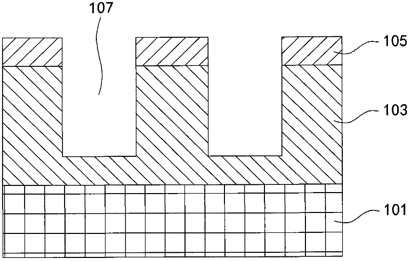
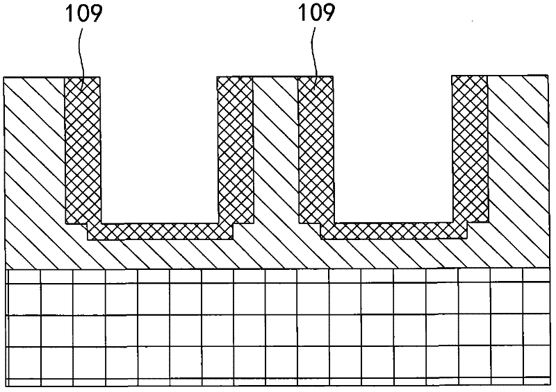
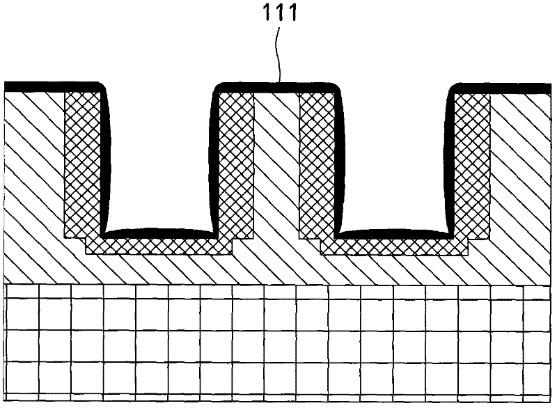
[0069] Figures 1A-1G is a cross-sectional view of a semiconductor structure illustrating a method of fabricating a semiconductor structure with an air gap region according to a conventional method.

[0070] refer to Figure 1A , a partially fabricated integrated circuit include...


PUM

PropertyMeasurementUnit
thicknessaaaaaaaaaa
thicknessaaaaaaaaaa
thicknessaaaaaaaaaa

Abstract

The invention provides a semiconductor structure, a method for manufacturing the semiconductor structure and a method for manufacturing a light cover with an air-gap region. The semiconductor structure includes a first metal-containing layer, a dielectric capping layer, a second metal-containing layer, and a conductive pad. The first metal-containing layer includes a set of metal structures, a dielectric filler disposed to occupy a portion of the first metal-containing layer, and an air-gap region defined by at least the set of metal structures and the dielectric filler and abutting at least a portion of the set of metal structures. The second metal-containing layer includes at least a via plug electrically connected to a portion of the set of metal structures. The conductive pad and the via plug do not overlap the air-gap region.

Description

technical field [0001] One or more embodiments of the present invention relate to integrated circuits, and more particularly to a semiconductor structure having an air-gap region and a method of manufacturing the same. Background technique [0002] Typically, the semiconductor manufacturing process is divided into two main stages: a front-end process stage (front-end process stage) and a back-end-of-line (BEOL) process stage. The preceding process refers to the formation of electronic components and / or electronic components on a semiconductor substrate, such as transistors, such as resistors and capacitors. On the other hand, the back-end process refers to the formation of metal interconnections between different electronic components and electronic components to realize the designed circuit. Typically, the layers of the metal interconnect are electrically insulated by an insulating dielectric material, such as silicon oxide or silicate glass. [0003] Generally, as the de...

Claims


Application Information

Patent Timeline
Patent Type & Authority Applications(China)
IPC IPC(8): H01L23/522H01L23/532H01L21/762H01L21/768
CPCH01L2924/0002H01L23/53295H01L21/02203H01L2924/12044H01L23/5329H01L23/5222H01L21/7682H01L21/76814H01L21/76826H01L2221/1063H01L2924/00H01L21/76805H01L21/76834H01L21/76897H01L23/5226H01L23/53238
Inventor 苏淑慧黄震麟杨景峰吴振诚吴仁贵陈殿豪米玉杰
Owner TAIWAN SEMICON MFG CO LTD
Why Eureka
Try Eureka