Method for controlling growing lengths of silicon nanowires
A technology of silicon nanowires and silicon wafers, which is applied in the field of nanomaterial preparation, can solve the problems such as difficulty in forming silicon nanowires with large aspect ratios, and achieve the effects of low cost, simple and reliable process, and short growth time
- Summary
- Abstract
- Description
- Claims
- Application Information
AI Technical Summary
Problems solved by technology
Method used
Image

Examples
Embodiment 1
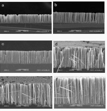
[0017] a. Take an N-type 100-crystal double-sided polished silicon wafer with a size of 0.5×0.5cm, and use the RCA standard cleaning process to clean it;
[0018] b. Weighing AgNO 3 0.595g, dissolve it in 50ml deionized water, and ultrasonically oscillate to make it fully dissolved to obtain a silver nitrate solution; the configured silver nitrate solution and the hydrofluoric acid solution with a concentration of 40% are in a volume ratio of 1:1 Mix evenly to obtain 100ml of etchant;
[0019] c. Set the temperature of the water bath to 20°C, put the plastic reactor containing the above-mentioned etchant solution into the water bath, and put the cleaned double-sided polished silicon wafer into the plastic reactor when the temperature is stable;
[0020] d. Take it out after reacting for 1 hour, put it into a nitric acid solution with a concentration of 65-68% and react for 30 seconds, remove the silver on the surface of the silicon wafer, then wash it with deionized water, d...
Embodiment 2
[0022] a. Take N-type 100 crystal orientation, double-sided polished silicon wafer with a size of 1×1cm, and use RCA standard cleaning process for cleaning;
[0023] b. Weighing AgNO 3 0.595g, dissolve it in 50ml deionized water, and ultrasonically oscillate to make it fully dissolved to obtain a silver nitrate solution; the configured silver nitrate solution and the hydrofluoric acid solution with a concentration of 40% are in a volume ratio of 1:1 Mix evenly to obtain 100ml of etchant;
[0024] c. Set the temperature of the water bath to 30°C, put the plastic reactor containing the above-mentioned etchant solution into the water bath, and put the cleaned double-sided polished silicon wafer into the plastic reactor when the temperature is stable;
[0025] d. Take it out after reacting for 1 hour, put it into a nitric acid solution with a concentration of 65-68% and react for 30 seconds, remove the silver on the surface of the silicon wafer, then wash it with deionized water...
Embodiment 3
[0027] a. Take an N-type 100-crystal double-sided polished silicon wafer with a size of 0.7×0.7cm, and use the RCA standard cleaning process for cleaning;
[0028] b. Weighing AgNO 3 0.595g, dissolve it in 50ml deionized water, and ultrasonically oscillate to make it fully dissolved to obtain a silver nitrate solution; the configured silver nitrate solution and the hydrofluoric acid solution with a concentration of 40% are in a volume ratio of 1:1 Mix evenly to obtain 100ml of etchant;
[0029] c. Set the temperature of the water bath to 40°C, put the plastic reactor containing the above-mentioned etchant solution into the water bath, and put the cleaned double-sided polished silicon wafer into the plastic reactor when the temperature is stable ;
[0030] d. Take it out after reacting for 1 hour, put it into a nitric acid solution with a concentration of 65-68% and react for 30 seconds, remove the silver on the surface of the silicon wafer, then wash it with deionized water...
PUM
 Abstract
Description
Claims
Application Information
 - R&D
- Intellectual Property
- Life Sciences
- Materials
- Tech Scout
- Unparalleled Data Quality
- Higher Quality Content
- 60% Fewer Hallucinations
Browse by: Latest US Patents, China's latest patents, Technical Efficacy Thesaurus, Application Domain, Technology Topic, Popular Technical Reports.
© 2025 PatSnap. All rights reserved.Legal|Privacy policy|Modern Slavery Act Transparency Statement|Sitemap|About US| Contact US: help@patsnap.com