Trench type MOSFET (metal-oxide-semiconductor field effect transistor) device

A trench gate and device technology, applied in the field of trench gate MOSFET devices, can solve problems such as large forward voltage drop, large resistance, and runaway, and achieve the effect of reducing impact, improving UIS performance, and small voltage drop

Inactive Publication Date: 2011-09-14
CHENGDU MONOLITHIC POWER SYST
View PDF5 Cites 6 Cited by
  • Summary
  • Abstract
  • Description
  • Claims
  • Application Information

AI Technical Summary

Problems solved by technology

Since the P-type body region is lightly doped, its resistance is large, so the forward voltage drop is also large, which is greater than the base-emitter turn-on voltage drop V of the equivalent parasitic transistor B BEon , so that the parasitic transistor B is turned on, and the current is amplified, resulting in runaway
At this point, the gate voltage will no longer be able to turn off the MOSFET device, making the MOSFET device permanently damaged

Method used


Image

  • Trench type MOSFET (metal-oxide-semiconductor field effect transistor) device
  • Trench type MOSFET (metal-oxide-semiconductor field effect transistor) device
  • Trench type MOSFET (metal-oxide-semiconductor field effect transistor) device

Examples


Embodiment Construction

[0020] Hereinafter, the present invention will be described in more detail with reference to the accompanying drawings. In the various figures, identical elements are indicated with similar reference numerals. For the sake of clarity, various parts in the drawings have not been drawn to scale.

[0021] The novel trench gate MOSFET device of the embodiment of the present invention will be described in detail below. In the following description, some specific details, such as specific doping types in the embodiments, are used to provide a better understanding of the embodiments of the present invention. It will be understood by those skilled in the art that embodiments of the invention may be practiced even without some details or other combinations of methods, materials, and the like.

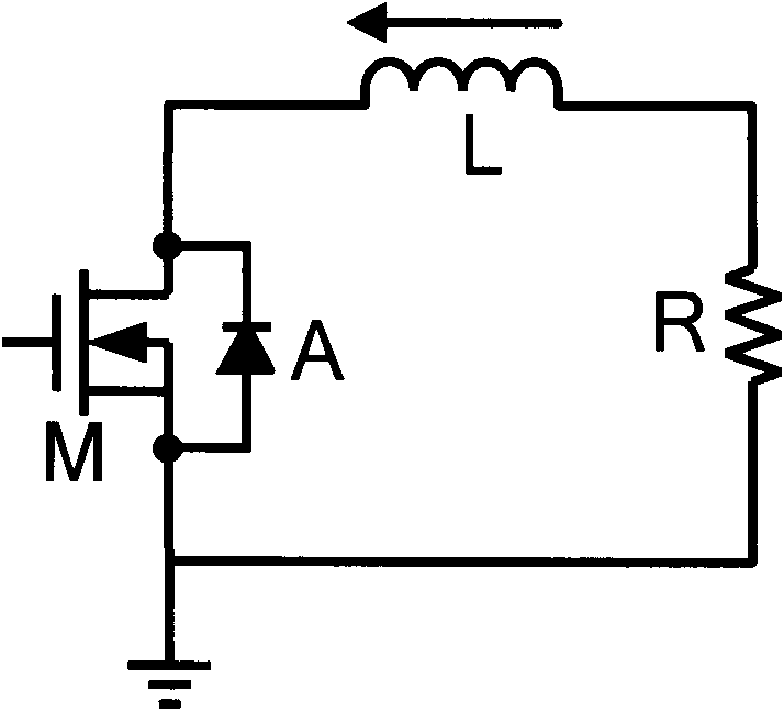
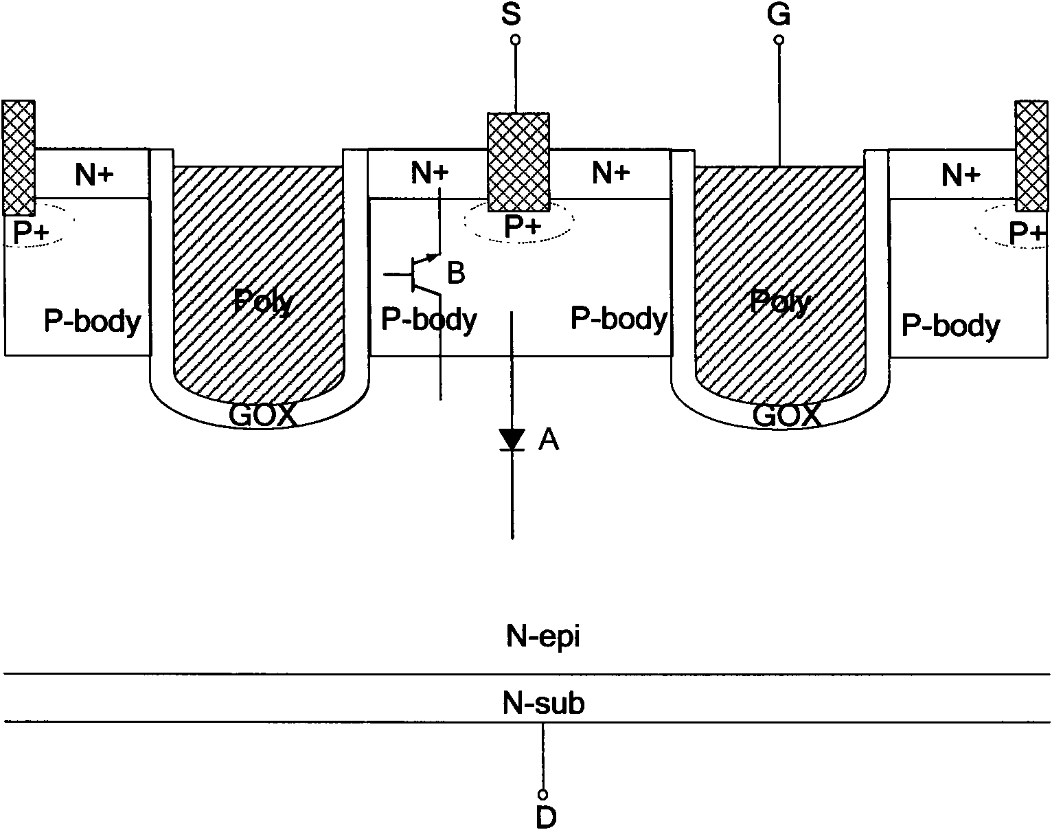
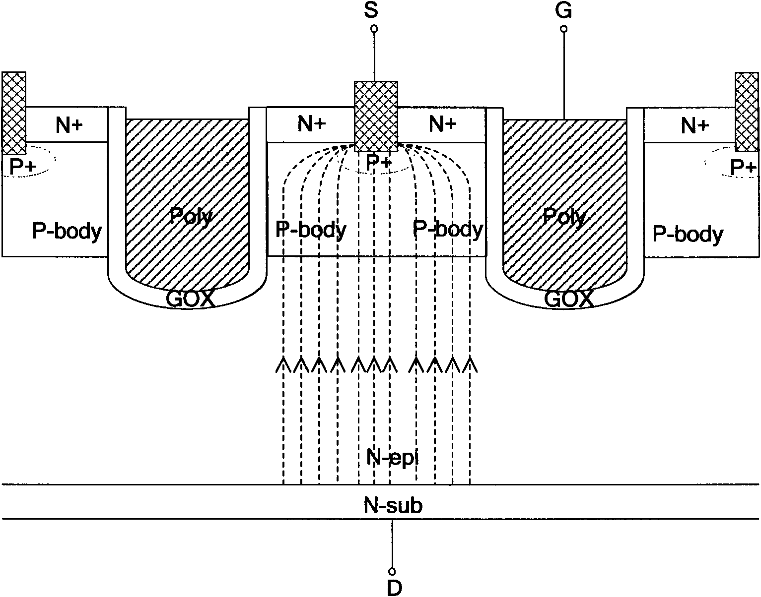
[0022] The invention proposes a novel trench gate metal oxide semiconductor field effect transistor (MOSFET) device. The unclamped inductive switch (UIS) performance of the trench gate MOSFET...


PUM


Abstract

The invention discloses a novel trench type MOSFET (metal-oxide-semiconductor field effect transistor) device and a manufacturing method thereof. A concave interface is formed between a body area and a semiconductor substrate, so that the part under source metal contact, of the body area is thinner than other parts of the body area. The most concave position E of the concave interface is positioned under the source metal contact so as to lead a reversed electric field to be gathered at the most concave position. A heavily doped region positioned under the source metal contact also can be formed in the body area so as to reduce the resistance. When the MOSFET is shut off, a reverse current is generated, flows through the heavily doped region from the most concave position and reaches the source metal contact, so that the influence of an equivalent parasitic transistor B on the shutoff of the MOSFET is reduced and the lower voltage drop is generated. In the novel trench type MOSFET device disclosed by the invention, the parasitic transistor is effectively controlled, and the UIS performance of the trench type MOSFET is improved.

Description

technical field [0001] The present invention relates to a MOSFET device, more specifically, to a trench gate MOSFET device. Background technique [0002] Trench-gate metal-oxide-semiconductor field-effect transistor (MOSFET) devices are widely used in the field of power management due to their high performance and low cost. When trench gate MOSFET devices are used in circuits with inductive loads, their unclamped inductive switching (UIS) performance is an important parameter affecting the performance of trench gate MOSFET devices. [0003] Such as figure 1 As shown, when the MOSFET M is turned on, the inductor L discharges through the MOSFET M. When the MOSFET M is turned off, since the inductor current cannot change suddenly, the parasitic diode A in the MOSFET M is broken down, and the inductor current is discharged through the parasitic diode A. UIS means that when the output terminal of the MOSFET is connected with an inductive device that cannot be clamped by other ...

Claims


Application Information

Patent Timeline
Patent Type & Authority Applications(China)
IPC IPC(8): H01L29/423H01L29/78H01L21/336H01L21/28
CPCH01L21/2652H01L29/41766H01L29/7805H01L21/266H01L29/1095H01L29/66727H01L29/66734H01L29/7813
Inventor 张磊唐纳德·R·迪斯尼李铁生马荣耀
Owner CHENGDU MONOLITHIC POWER SYST
Why Eureka
Try Eureka