Plane type VDMOS production method
A planar and N-type technology, applied in semiconductor/solid-state device manufacturing, electrical components, circuits, etc., to solve problems such as switching speed reduction, planar VDMOS threshold voltage drift, planar VDMOS failure, etc.
- Summary
- Abstract
- Description
- Claims
- Application Information
AI Technical Summary
Problems solved by technology
Method used
Image

Examples
Embodiment Construction
[0053] In order to make the purpose, technical solutions and advantages of the embodiments of the present invention clearer, the technical solutions in the embodiments of the present invention will be clearly and completely described below in conjunction with the drawings in the embodiments of the present invention. Obviously, the described embodiments It is a part of embodiments of the present invention, but not all embodiments. Based on the embodiments of the present invention, all other embodiments obtained by persons of ordinary skill in the art without making creative efforts belong to the protection scope of the present invention.
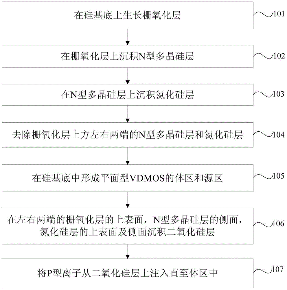
[0054] figure 2 It is a flow chart of Embodiment 1 of the manufacturing method of the planar VDMOS of the present invention, such as figure 2 As shown, the manufacturing method of the planar VDMOS provided in this embodiment includes:
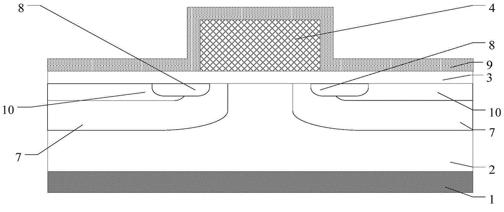
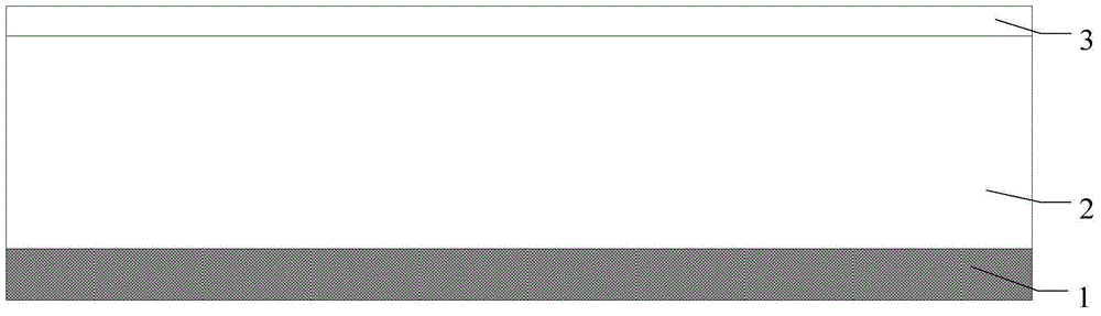
[0055] Step 101 , growing a gate oxide layer 3 on a silicon substrate.
[0056]In this embodiment, the...
PUM
| Property | Measurement | Unit |
|---|---|---|
| Thickness | aaaaa | aaaaa |
Abstract
Description
Claims
Application Information
 - R&D
- Intellectual Property
- Life Sciences
- Materials
- Tech Scout
- Unparalleled Data Quality
- Higher Quality Content
- 60% Fewer Hallucinations
Browse by: Latest US Patents, China's latest patents, Technical Efficacy Thesaurus, Application Domain, Technology Topic, Popular Technical Reports.
© 2025 PatSnap. All rights reserved.Legal|Privacy policy|Modern Slavery Act Transparency Statement|Sitemap|About US| Contact US: help@patsnap.com