Method for improving power metal oxide semiconductor (MOS) device unclamped inductive switching (UIS) performance
A MOS device and performance technology, applied in semiconductor/solid-state device manufacturing, electrical components, circuits, etc., can solve problems such as device failure, achieve the effects of reducing turn-on, improving UIS performance, and improving UIS performance
- Summary
- Abstract
- Description
- Claims
- Application Information
AI Technical Summary
Problems solved by technology
Method used
Image

Examples
Embodiment Construction
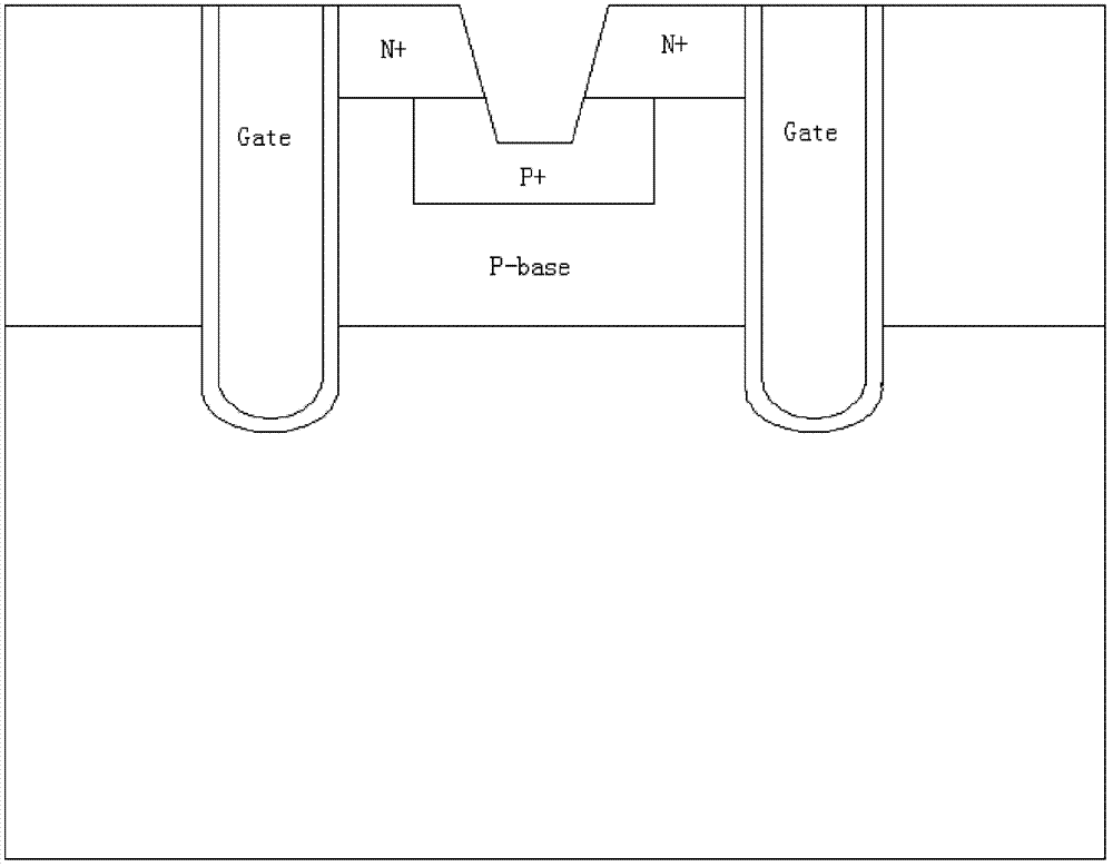
[0022] The method for improving the UIS performance of the PowerMOS device of the present invention includes:
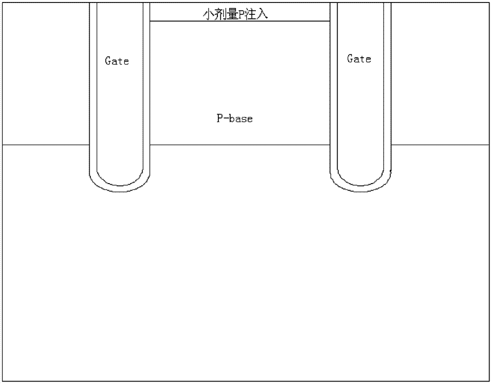
[0023] (1) On the basis of the preparation process of the existing power MOS device, a large dose of source implantation (N-type impurity implantation) at the original PowerMOS source end was changed to 10 13 ~10 14 cm -2 A small dose of P-source implantation to form N-source, and a 4 × 10 15 ~8×10 15 cm -2 A large dose of As source is implanted to form N+source;
[0024] Among them, the schematic diagram of the structure after the first source injection, such as image 3 As shown, it can be seen that compared with ordinary products, the structure is basically the same, but the N-type impurity concentration of the first source injection is smaller, and this step is used to form a deeper N-source;
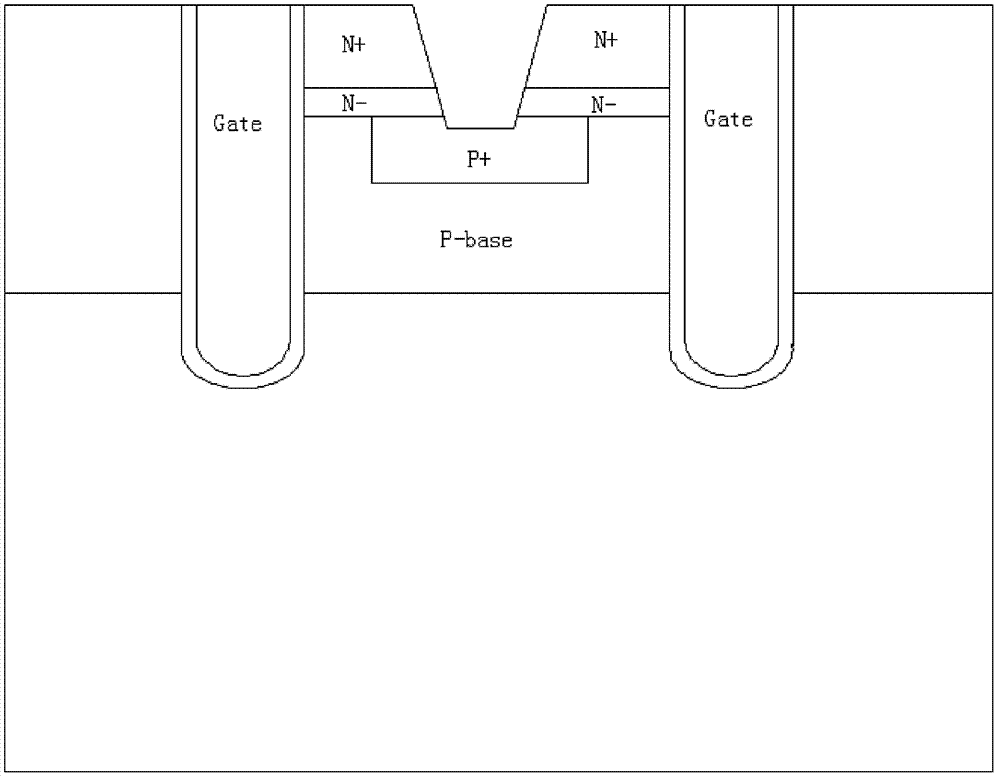
[0025] Schematic diagram of the structure after the second source injection, such as Figure 4 As shown, it can be seen that compared with the existing (traditional...
PUM
 Abstract
Description
Claims
Application Information
 - R&D
- Intellectual Property
- Life Sciences
- Materials
- Tech Scout
- Unparalleled Data Quality
- Higher Quality Content
- 60% Fewer Hallucinations
Browse by: Latest US Patents, China's latest patents, Technical Efficacy Thesaurus, Application Domain, Technology Topic, Popular Technical Reports.
© 2025 PatSnap. All rights reserved.Legal|Privacy policy|Modern Slavery Act Transparency Statement|Sitemap|About US| Contact US: help@patsnap.com