Detector material for a detector for use in ct systems, detector element and detector

A technology of detectors and components, applied in the direction of electrical components, electric solid-state devices, semiconductor devices, etc., can solve the problem of large detectable flux of direct conversion detectors, failure to prevent polarization effects of direct conversion detectors, and inability to measure, etc. problem, to achieve the effect of enhancing signal stability and measurement repeatability

Inactive Publication Date: 2014-06-25
SIEMENS AG
View PDF5 Cites 0 Cited by
  • Summary
  • Abstract
  • Description
  • Claims
  • Application Information

AI Technical Summary

Problems solved by technology

Polarization is therefore limiting in the maximum detectable throughput of direct conversion detectors
[0005] Currently, none of the solutions known in the prior art prevent polarization effects in direct conversion detectors
That is, it is currently not possible to measure higher radiation fluxes such as occur in CT systems with direct conversion detectors

Method used


Image

  • Detector material for a detector for use in ct systems, detector element and detector
  • Detector material for a detector for use in ct systems, detector element and detector
  • Detector material for a detector for use in ct systems, detector element and detector

Examples


Embodiment Construction

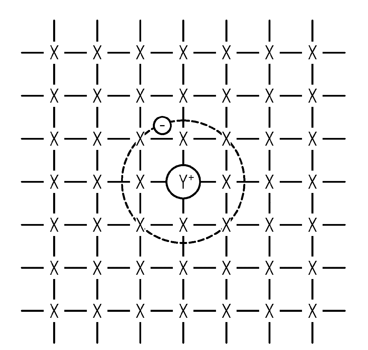
[0032] figure 1 A schematic diagram of a semiconductor doped with a donor atom. The atoms of the semiconductor crystal are marked X, and the donor atoms are marked Y. The bonds between these atoms are indicated by dashes. In this general example, the donor atom is located at the normal atomic position in the semiconductor crystal, thereby displacing a semiconductor atom. According to the relevant definition of the donor atom, the donor atom releases a weakly bound electron into the conduction band. That is, the donor atoms are ionized. Meanwhile, the donor atom's positively charged nucleus stays in place.

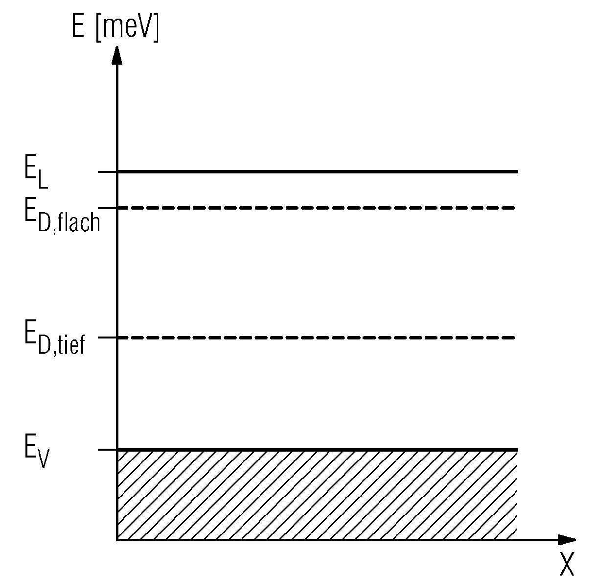
[0033] As a specific example of semiconductor doping in the present invention, CdTe semiconductor is doped with chlorine. The Cl concentration of conventional CdTe:Cl detectors for detecting gamma radiation and X-ray radiation is about 1*10 17 / cm 3 up to 2*10 17 / cm 3 . Such detectors are not suitable for high-throughput applications due to the strong polarizatio...


PUM


Abstract

A detector material for a detector is disclosed for use in CT systems, particularly in dual-energy CT systems, including a doped semiconductor. In at least one embodiment, the semiconductor is doped with a donator in a concentration, wherein the concentration of the donator corresponds to at least 50% of the maximum solubility thereof in the semiconductor material, and the donator produces flat imperfections having an excitation energy. The flat imperfections can be ionized and can provide additional freely moveable charge carriers. The freely moveable charge carriers can be captured by the spatially separated deep imperfections and thus reduce the number of the charged deep imperfections. In this way, pure time- and radiation-dependent effects, such as polarization, occur more often. The invention further more relates to the use of the detector material in a CT or dual-energy CT system for generating tomographic images of a test object.

Description

technical field [0001] The invention relates to a detector material for a detector used in a CT system, in particular a dual-energy CT system, the detector material consists of a semiconductor doped with a donor (Donator). The invention furthermore relates to a detector with a plurality of detector elements, using the above-mentioned detector material. Background technique [0002] To detect gamma and X-ray radiation, especially in CT systems and dual-energy CT systems, conventional methods mainly use direct-conversion detectors based on semiconductor materials such as CdTe, CdZnTe, CdTeSe, and CdZnTeSe. These materials need to be doped in order to produce the electrical properties required for the detector to work. Doping is usually performed with one element of Cl, In and Al or a combination of at least one element of the third main group of the periodic table and at least one element of the eighth subgroup of the periodic table. [0003] The growth processes of semicond...

Claims


Application Information

Patent Timeline
Patent Type & Authority Patents(China)
IPC IPC(8): H01L27/146H01L31/115
CPCH01L27/14659H01L31/115H01L31/0296
Inventor 彼得·哈肯施米德马蒂亚斯·施特拉斯堡
Owner SIEMENS AG
Why Eureka
Try Eureka