Solution and method for displaying outline of electrostatics discharge (ESD) positive-negative (PN) junction in power metal oxide semiconductor (MOS)

A solution and profile technology, applied in the preparation of test samples, scanning probe technology, instruments, etc., can solve the problem that the ESDPN junction profile in power MOS cannot be clearly displayed, and achieve the effect of less damage

Active Publication Date: 2011-09-21
SEMICON MFG INT (SHANGHAI) CORP +1
View PDF6 Cites 6 Cited by
  • Summary
  • Abstract
  • Description
  • Claims
  • Application Information

AI Technical Summary

Problems solved by technology

[0005] The object of the present invention is to provide a solution and method for developing the outline of the ESD PN junction in the power MOS

Method used


Image

  • Solution and method for displaying outline of electrostatics discharge (ESD) positive-negative (PN) junction in power metal oxide semiconductor (MOS)
  • Solution and method for displaying outline of electrostatics discharge (ESD) positive-negative (PN) junction in power metal oxide semiconductor (MOS)
  • Solution and method for displaying outline of electrostatics discharge (ESD) positive-negative (PN) junction in power metal oxide semiconductor (MOS)

Examples


Embodiment Construction

[0016] In order to make the purpose and features of the present invention more comprehensible, the specific implementation manners of the present invention will be further described below in conjunction with the accompanying drawings.

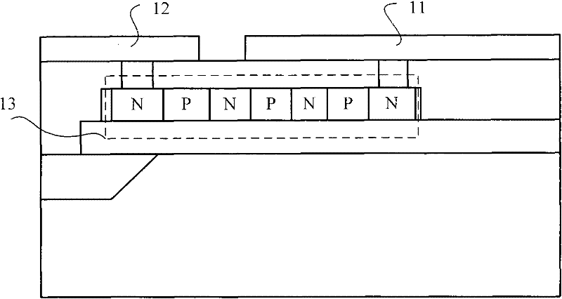
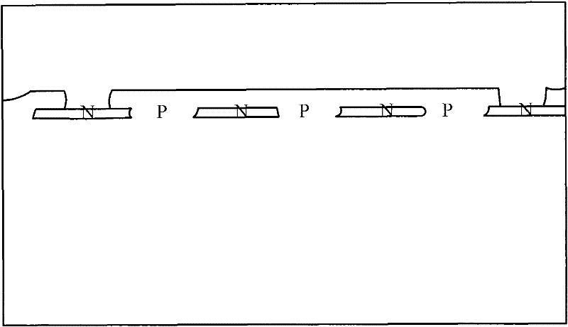
[0017] It has been mentioned in the background art that when the traditional contour visualization solution is applied to the ESDPN junction in the power MOS, the contour of the junction cannot be clearly visualized.

[0018] The solution for developing the outline of the ESD PN junction in the power MOS of the present invention includes an HF solution with a mass percent concentration of 49% and a mass percent concentration of 70% HNO 3 solution, the HF solution and HNO 3 The volume ratio of the solution ranges from 1:300 to 5:100. Among them, HNO 3 As an oxidizing agent (oxidizing agent), and HF as a complexing agent (complexing agent). The oxidizing agent reacts silicon to silicon oxide, and the complexing agent reacts with silicon oxide....


PUM


Abstract

The invention discloses a solution and a method for displaying an outline of an electrostatics discharge (ESD) positive-negative (PN) junction in a power metal oxide semiconductor (MOS). In the method, the solution for displaying the outline is prepared from a 49 mass percent HF solution and a 70 mass percent HNO3 solution in a volume ratio of (1:300)-(5:100), and a sample to be detected is soaked in the solution for displaying the outline for preset time, and is reacted with an N+ region to slightly damage a P+ region, so that the outline of the ESD PN junction in the power MOS is displayed clearly. Moreover, the method for displaying the outline is simple and is convenient to operate, and the outline which is damaged slightly is provided so as to facilitate the subsequent scanning electron microscope (SEM) analysis of devices.

Description

technical field [0001] The invention relates to the technical field of semiconductor device testing, in particular to a solution and method for developing the contour of an ESD PN junction in a power MOS. Background technique [0002] During the manufacturing process and the final system application process, an electrostatic discharge (ESD) phenomenon may occur in the integrated circuit. ESD phenomena typically cause the discharge of high voltage potentials (typically thousands of volts) resulting in short-term (typically 100 ns) high current (several amps) pulses, which can destroy fragile devices present in current integrated circuits, resulting in functional failure of the system. Therefore, ESD protection is essential for integrated circuits. [0003] The current improved metal oxide semiconductor field effect transistor (MOSFET) usually forms an electrical protection structure to prevent static electricity accumulation and discharge. For example, adding a resistor bet...

Claims


Application Information

Patent Timeline
IPC IPC(8): G01N1/28G01Q30/02
Inventor 余萍洪春雷范启义
Owner SEMICON MFG INT (SHANGHAI) CORP
Why Eureka
Try Eureka