
P-type epitaxial layer-based binary coded decimal (BCD) integrated device and manufacturing method thereof

A technology of integrated devices and epitaxial layers, applied in semiconductor/solid-state device manufacturing, electric solid-state devices, semiconductor devices, etc., can solve the problems of increasing the cost of chip manufacturing and increasing the cost of silicon wafers, so as to reduce the cost of chip manufacturing and reduce the complexity of the process. to achieve the effect of self-isolation

Inactive Publication Date: 2011-09-21
UNIV OF ELECTRONICS SCI & TECH OF CHINA
View PDF5 Cites 21 Cited by
  • Summary
  • Abstract
  • Description
  • Claims
  • Application Information

AI Technical Summary

Problems solved by technology

In order to improve the vertical body withstand voltage of the device, high-resistivity silicon wafers are usually used as substrates, but high-resistance wafers (>100Ω·cm) are usually manufactured by zone melting, which increases the cost of silicon wafers and increases chip manufacturing costs.

Method used


Image

  • P-type epitaxial layer-based binary coded decimal (BCD) integrated device and manufacturing method thereof
  • P-type epitaxial layer-based binary coded decimal (BCD) integrated device and manufacturing method thereof
  • P-type epitaxial layer-based binary coded decimal (BCD) integrated device and manufacturing method thereof

Examples


Embodiment Construction

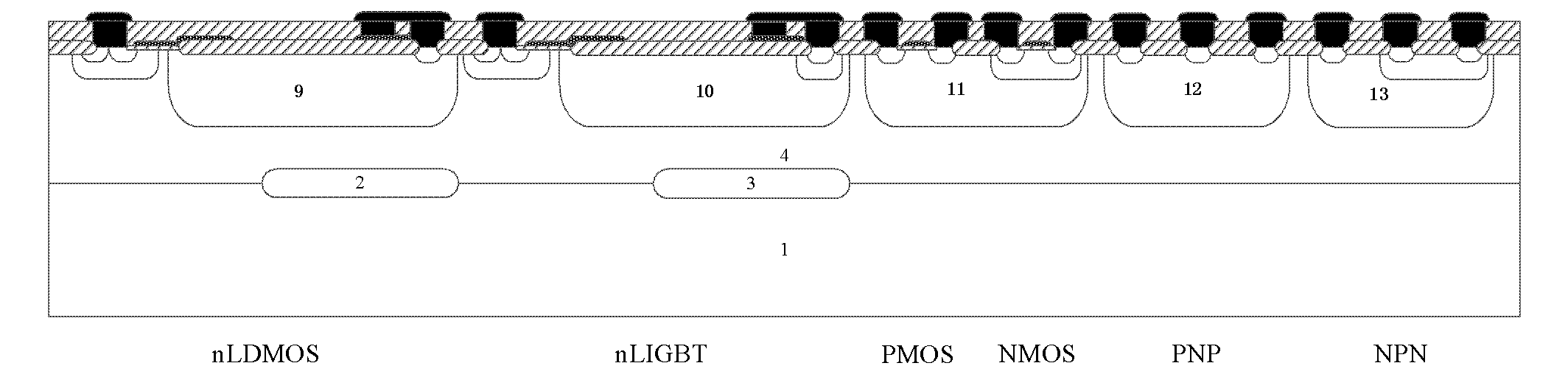
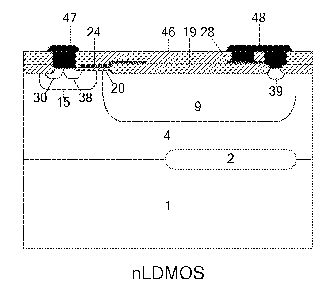
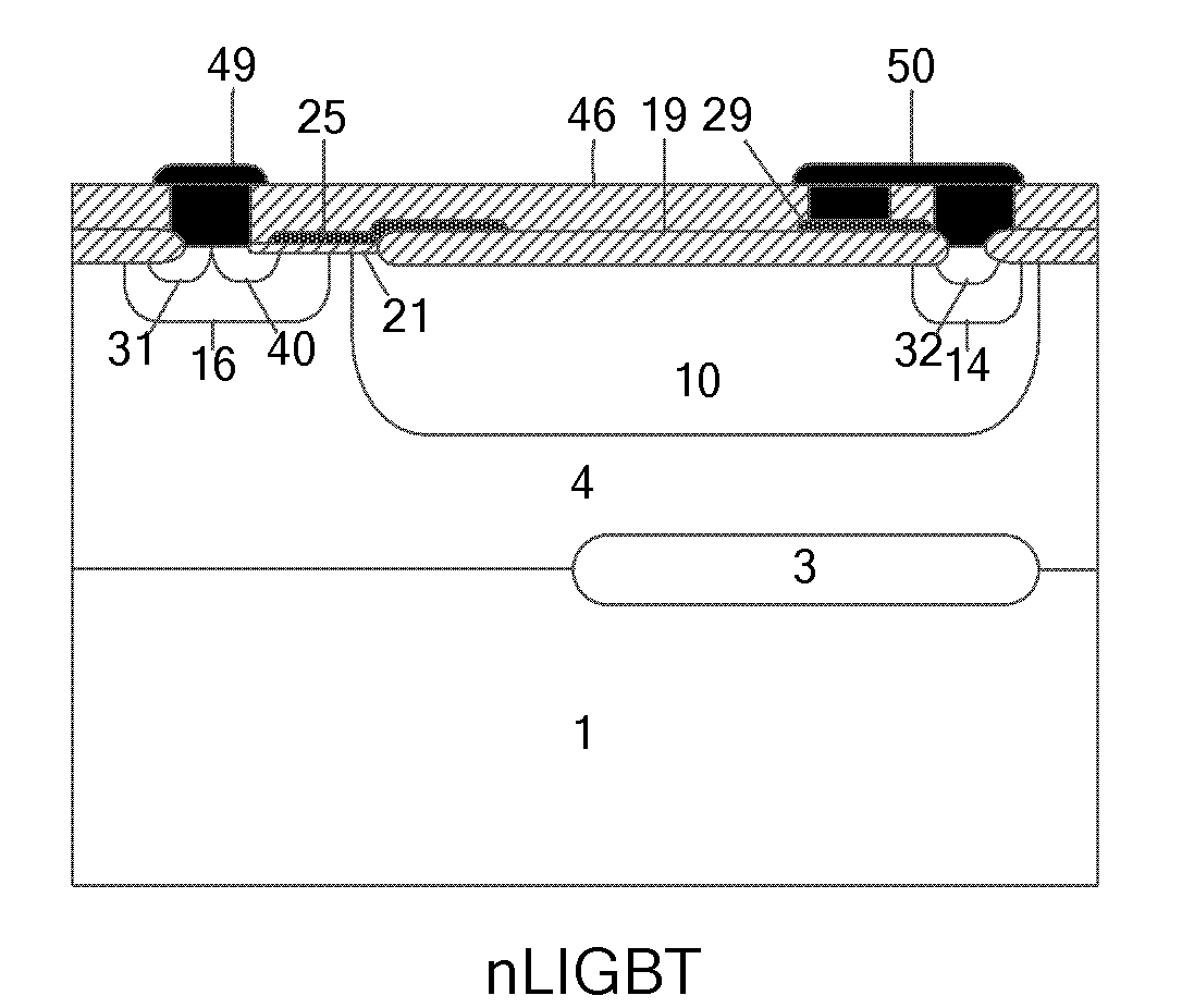
[0025] The invention provides a BCD integrated device based on a P-type epitaxial layer, such as figure 1 As shown, it includes high-voltage nLDMOS devices, high-voltage nLIGBT devices, low-voltage PMOS devices, low-voltage NMOS devices, low-voltage PNP devices, and low-voltage NPN devices integrated on the same P-type substrate 1. The high-voltage nLDMOS devices, high-voltage nLIGBT devices, low-voltage PMOS devices, low-voltage NMOS devices, low-voltage PNP devices, and low-voltage NPN devices are fabricated in the P-type epitaxial layer 4 on the surface of the P-type substrate, and the P-type epitaxial layer 4 is used to form between the devices Self-isolation; there is a first N-type buried layer 2 between the P-type substrate 1 and the P-type epitaxial layer 4 under the high-voltage nLDMOS device, and between the P-type substrate 1 and the P-type epitaxial layer 4 under the high-voltage nLIGBT device There is a second N-type buried layer 3 in between.

[0026] The present in...


PUM


Abstract

The invention discloses a P-type epitaxial layer-based binary coded decimal (BCD) integrated device and a manufacturing method thereof and belongs to the technical field of semiconductor power devices. A high-voltage n laterally diffused metal oxide semiconductor (LDMOS) device, a high-voltage n lateral insulated gate bipolar transistor (LIGBT) device, a low-voltage P-channel metal oxide semiconductor (PMOS) device, a low-voltage N-channel metal oxide semiconductor (NMOS) device, a low-voltage plug-and-play (PNP) device and a low-voltage negative-positive-negative (NPN) device are integrated on the same substrate; various devices are manufactured in a P-type epitaxial layer on the surface of a P-type substrate and are self-isolated through the P-type epitaxial layer; an N-type buried layer is formed between the P-type substrate below a high-voltage device and the P-type epitaxial layer; and the N-type buried layer can (or cannot) be formed on the P-type epitaxial layer on two sides below a low-voltage device. Due to the introduction of the N-type buried layer, a lower-resistivity silicon chip can be used as a substrate under the same breakdown voltage, and increase of chip manufacturing cost brought by a manufactured monocrystalline silicon chip by a floating zone (FZ) method is avoided; therefore, the manufacturing cost of the chip is reduced.

Description

Technical field [0001] The invention belongs to the technical field of semiconductor power devices. Background technique [0002] BCD (Bipolar CMOS DMOS) process technology utilizes the high analog accuracy of Bipolar transistors, the high integration of CMOS and the high power characteristics of DMOS (Double-diffused MOSFET) to realize Bipolar analog circuits, CMOS logic circuits, CMOS analog circuits and DMOS high voltage Monolithic integration of power devices. Lateral high voltage power devices LDMOS (Lateral Double-diffused MOSFET) and LIGBT (Lateral Insulated Gate Bipolar Trasistor) are easily compatible with traditional CMOS devices, so they have been widely used in the field of smart power integrated circuits. The primary purpose of the design of the horizontal high-voltage power device is to achieve the rated breakdown voltage under a given drift zone length, and its breakdown voltage is determined by the lowest value of the lateral surface withstand voltage and the lon...

Claims


Application Information

Patent Timeline
Patent Type & Authority Applications(China)
IPC IPC(8): H01L27/06H01L21/8249H01L29/78H01L29/06
Inventor 乔明银杉赵远远何逸涛胡曦王猛庄翔
Owner UNIV OF ELECTRONICS SCI & TECH OF CHINA
Learn More