Semiconductor device and manufacturing method thereof

A semiconductor and device technology, which is applied to high-k/metal gate asymmetric semiconductor devices and their manufacturing fields, can solve problems such as driving current reduction, and achieve the effect of improving control ability and reducing EOT

Active Publication Date: 2011-09-21
INST OF MICROELECTRONICS CHINESE ACAD OF SCI
View PDF4 Cites 5 Cited by
  • Summary
  • Abstract
  • Description
  • Claims
  • Application Information

AI Technical Summary

Problems solved by technology

This allows the drive current of the device to be reduced

Method used


Image

  • Semiconductor device and manufacturing method thereof
  • Semiconductor device and manufacturing method thereof
  • Semiconductor device and manufacturing method thereof

Examples


no. 1 example

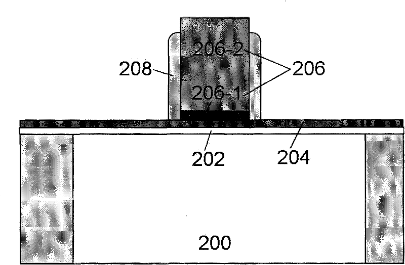
[0017] According to the first embodiment of the present invention, refer to figure 1 , figure 1 A flowchart showing a method of manufacturing a semiconductor device according to an embodiment of the present invention. In step S101, a semiconductor substrate is provided, referring to figure 2 . In the present invention, the substrate 200 includes a silicon substrate (such as a wafer) in a crystal structure, and the substrate 200 may also include other basic semiconductors or compound semiconductors, such as Ge, GeSi, GaAs, InP, SiC, or diamond. The substrate 200 may include various doping configurations according to design requirements known in the art (eg, p-type substrate or n-type substrate). Further, optionally, the substrate 200 may include epitaxial layers, may be altered by stress to enhance performance, and may include a silicon-on-insulator (SOI) structure.

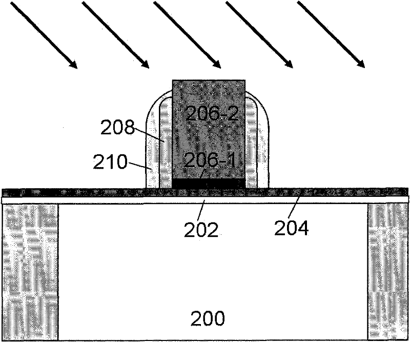
[0018] In steps S102 and S103, a gate stack 300 is formed on the semiconductor substrate 200, the gate sta...

no. 2 example

[0029] Only the aspects of the second embodiment that differs from the first embodiment will be described below. Parts not described should be considered to be performed using the same steps, methods or processes as those in the first embodiment, so details will not be repeated here.

[0030] According to the second embodiment of the present invention, refer to Figure 10 , Figure 10 A flow chart of a method for manufacturing a common-source semiconductor device according to an embodiment of the present invention is shown. In step S202, the interface layer 202, the gate dielectric layer 204, the first gate layer 206-1, and the sacrificial layer 230 are sequentially formed on the semiconductor substrate 200, and the sacrificial layer 230 is photolithographically etched. Figure 12 .

[0031] Specifically, firstly, the interface layer 202, the gate dielectric layer 204, the first gate layer 206-1, the sacrificial layer 230, the first stop layer 232, and the second stop layer...


PUM


Abstract

The invention relates to a semiconductor device and a manufacturing method thereof. The device is provided with a metal lateral wall on the side wall of a grid electrode at one side of a drain electrode region; the metal lateral wall is made of metal, such as Ta, and the like and has an oxygen uptake effect, thereby effectively reducing EOT (Equivalent Oxide Thickness) at one side of the drain electrode region and further effectively promoting the controllability of short channel control. In addition, because the EOT at one side of a source electrode region is larger, carrier drift mobility of the device cannot be deteriorated. Besides, the non-symmetrical device can have a better driving property.

Description

technical field [0001] The present invention generally relates to a semiconductor device and a manufacturing method thereof, in particular to a high-k / metal gate asymmetric semiconductor device capable of reducing the thickness of an equivalent oxide layer on one side of a drain region and a manufacturing method thereof. Background technique [0002] At present, CMOS device gate engineering research centered on "high-k gate dielectric / metal gate" technology is the most representative core process in 32 / 22 nanometer technology, and related materials, processes and structures have been extensively studied. processing. Intel disclosed that after using a high-k gate dielectric material, the leakage current of the device is greatly reduced. However, in the high-k / metal gate process, due to the high-temperature annealing process must be used in the process integration process, the interface layer between the high-k dielectric material and the substrate becomes thicker during the ...

Claims


Application Information

Patent Timeline
Patent Type & Authority Applications(China)
IPC IPC(8): H01L29/78H01L29/43H01L21/336H01L21/28
CPCH01L29/7835H01L29/66659H01L29/6656H01L29/4983
Inventor 梁擎擎钟汇才朱慧珑
Owner INST OF MICROELECTRONICS CHINESE ACAD OF SCI
Why Eureka
Try Eureka