Device structure with channel-oxide-nanotube super junction and preparation method thereof

A device structure, nanotube technology, used in semiconductor/solid-state device manufacturing, semiconductor devices, diodes, etc.

Active Publication Date: 2011-09-21
ALPHA & OMEGA SEMICON INT LP
View PDF10 Cites 22 Cited by
  • Summary
  • Abstract
  • Description
  • Claims
  • Application Information

AI Technical Summary

Problems solved by technology

This solves the limitation of high R

Method used


Image

  • Device structure with channel-oxide-nanotube super junction and preparation method thereof
  • Device structure with channel-oxide-nanotube super junction and preparation method thereof
  • Device structure with channel-oxide-nanotube super junction and preparation method thereof

Examples


Embodiment Construction

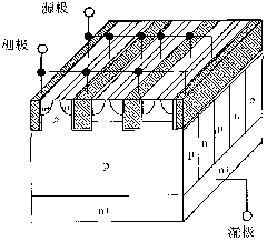
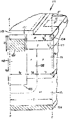
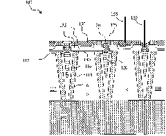
[0034] image 3 A cross-sectional view of a trenched nanotube metal oxide semiconductor field effect transistor (MOSFET) device 100 according to the present invention is shown. The MOSFET element is formed in a P-type epitaxial layer 110 on the N+ substrate 105 . A plurality of trenched nanotubes 115 and a plurality of trenches are formed in the epitaxial layer 110 . The trench sidewalls are slightly beveled to form a tapered trench. As an example, the side walls may be slightly sloped at 87-89 degrees. Each trench sidewall is covered by N+ epitaxial layer 115 . Another lightly doped P- epitaxial layer 116 is grown over N+ epitaxial layer 115 . Due to the remaining trench width and the slope angle of the trench, the sidewalls of the P- epitaxial layer 116 meet toward the bottom and fully fill the bottom of the trench. The remaining central portion of the trench is filled with a dielectric such as silicon oxide 120 . The MOSFET device 100 also includes a trench gate 130 f...


PUM


Abstract

The invention relates to a device structure with channel-oxide-nanotube super junction and a method for preparing the same and proposes a semiconductor power device precipitated on a first conductive type semiconductor substrate. The semiconductor substrate bears a second conductive type epitaxial layer, and the semiconductor power device is arranged on a super junction structure. The super junction structure comprises a plurality of grooves opened on the top face of the epitaxial layer, wherein the sidewalls of each of the grooves are covered with a first conductive type first epitaxial layer to neutralize the charge of the second conductive type epitaxial layer. The second conductive type epitaxial layer can be grown over the first epitaxial layer. Each of the groove is filled with a non-doped dielectric material in a remaining groove slot space. The sidewalls of each of the grooves have an angle of inclination to form a converged U-shaped groove.

Description

technical field [0001] The present invention generally relates to semiconductor power devices, more specifically, the present invention relates to the structure and preparation of trenched nanotubes with trenched sidewalls, wherein the trenched sidewalls are covered with a doped epitaxial layer and then covered with an insulating material The trench sidewalls are filled, so that a measurable charge-balanced semiconductor power device can be flexibly prepared with a simplified manufacturing process, and simultaneously high breakdown voltage and very low resistance can be obtained. Background technique [0002] Although there are a lot of patent information and published technical documents in order to improve the electrical characteristics of semiconductor devices with vertical super junction structures, there are still many technical difficulties and preparations in the related fields of design and preparation of super junction semiconductor devices. limited. More specifica...

Claims


Application Information

Patent Timeline
IPC IPC(8): H01L29/78H01L29/06H01L21/336H01L29/739H01L21/331
CPCH01L21/26586H01L29/06H01L29/0619H01L29/0634H01L29/0638H01L29/0649H01L29/0653H01L29/0661H01L29/0676H01L29/0692H01L29/0696H01L29/0878H01L29/0886H01L29/365H01L29/402H01L29/404H01L29/4236H01L29/42368H01L29/66136H01L29/66143H01L29/66325H01L29/66348H01L29/66477H01L29/66734H01L29/7393H01L29/7395H01L29/7397H01L29/78H01L29/7803H01L29/7806H01L29/7811H01L29/7813H01L29/7827H01L29/861H01L29/872
Inventor 哈姆扎·依玛兹马督儿·博德李亦衡管灵鹏王晓彬陈军安荷·叭剌
Owner ALPHA & OMEGA SEMICON INT LP
Why Eureka
Try Eureka