Organic semiconductor element and organic electrode

A technology of organic semiconductors and components, applied in semiconductor devices, semiconductor/solid-state device manufacturing, electrical components, etc.

Inactive Publication Date: 2011-09-21
RICOH KK +1
View PDF5 Cites 5 Cited by
  • Summary
  • Abstract
  • Description
  • Claims
  • Application Information

AI Technical Summary

Problems solved by technology

At present, realizing applications using organic semiconductors is a great challenge to be accomplished

Method used


Image

  • Organic semiconductor element and organic electrode
  • Organic semiconductor element and organic electrode
  • Organic semiconductor element and organic electrode

Examples


specific example

[0064] Specific examples of derivatives used in the present invention are as follows:

[0065]

[0066] These tetrathiafulvalene derivatives can be used independently or in combination according to conventional practice. These derivatives can be synthesized by synthetic methods known in the art. Also, those synthesized using the synthesis method proposed by the present inventors can be used (see Japanese Patent Application No. 2009-073990, No. 2010-000319 and No. 2010-026729, the disclosures of which are incorporated herein by reference).

[0067] For example, tetrathiafulvalene derivatives can be produced by subjecting 1,3-bisthiol-2-one compounds, which are raw materials, to a coupling reaction (see J. Org, Chem., 2000, 65, 5794-5805). In this case, the raw material 1,3-bisthiol-2-one compound can be obtained, for example, in the following manner. By the reactions disclosed in J.Org.Chem.1994,59,6519-6527, Chem.Commun.1998,361-362, Chem.Commun.1998,2197-2198, Tetrahedro...

Embodiment 1

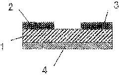
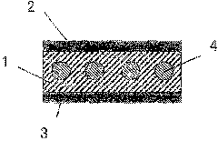
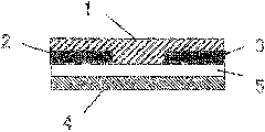
[0088] Prepared using bis(anthracene[2,3-d])tetrathiafulvalene (1) as follows Figure 1D An organic semiconductor element with an upper contact structure is shown.

[0089] An n-type silicon substrate provided with a thermally oxidized film having a thickness of 300 nm was washed by immersing the substrate in strong sulfuric acid for 24 hours. The washed silicon substrate was immersed in a toluene solution of a silane coupling agent (ie, octyltrichlorosilane) (1 mM), and subjected to ultrasonic treatment for 5 minutes to form a monomolecular film on the surface of the silicon oxide film.

[0090] On the substrate prepared above by vacuum evaporation (back pressure: up to 10 -4 Pa, deposition rate: , film thickness: 25 nm) bis(anthracene[2,3-d])tetrathiafulvalene (1) was deposited on the entire surface of the substrate to form a film, thereby forming a first organic compound layer. Thereafter, fullerenes were deposited by evaporation using a metal mask having an electrode...

Embodiment 2

[0097] The electrical characteristics of the organic semiconductor element prepared in Example 1 were evaluated in the same manner as in Example 1, except that the probing positions of the source and drain electrodes were changed to Figure 2B The probing position shown in 2. As a result, it was found that the organic semiconductor element exhibits the characteristics of a p-type organic thin film transistor. The current-voltage (I-V) characteristics of the organic thin film transistor are in Figure 4 shown in .

[0098] The electron field effect mobility of the organic thin film transistor is 0.005cm 2 / Vs.


PUM


Abstract

The invention provides an organic semiconductor element and an organic electrode. The organic semiconductor element contains: a source electrode containing a first organic compound layer and a second organic compound layer, at least one of the layers having an organic semiconductor active region; and a drain electrode containing the first organic compound layer and the second organic compound layer, as well as providing an organic electrode, containing: a laminated film, in which a layer of a tetrathiafulvalene derivative expressed by the following general formula I and a layer of an electron accepting compound are laminated.

Description

technical field [0001] The present invention relates to organic semiconductor elements and organic electrodes, which are expected to be applied to organic electronic devices such as organic conductors, organic superconductors, organic magnetic materials, organic thermoelectric elements, organic electrochromic elements and organic electroluminescent elements. Background technique [0002] Organic electronic devices have excellent flexibility and portability, so the practical value of organic electronic devices is expected to further increase. For this reason, development and research on devices that are main parts of organic electronic devices such as organic semiconductors, organic LEDs, and organic solar cells have been actively conducted. Organic materials are inherently insulating, so metals are used in most electrode areas in these devices. Therefore, in order to utilize the properties of organic compounds such as flexibility and portability, it is desirable to develop ...

Claims


Application Information

Patent Timeline
Patent Type & Authority Applications(China)
IPC IPC(8): H01L51/44H01L51/46H01L51/52H01L51/54
CPCB82Y10/00H01L51/0074H01L51/0562H01L51/102H01L51/0045H01L51/0051H10K85/20H10K85/611H10K85/6576H10K10/486H10K10/82H10K10/84
Inventor 加藤拓司山本谕匂坂俊也田野隆德篠田雅人后藤大辅松本真二毛利匡贵油谷圭一郎安达千波矢鸟居昌史
Owner RICOH KK
Why Eureka
Try Eureka